


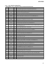
89
HCD-PX333
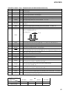
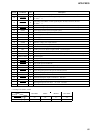
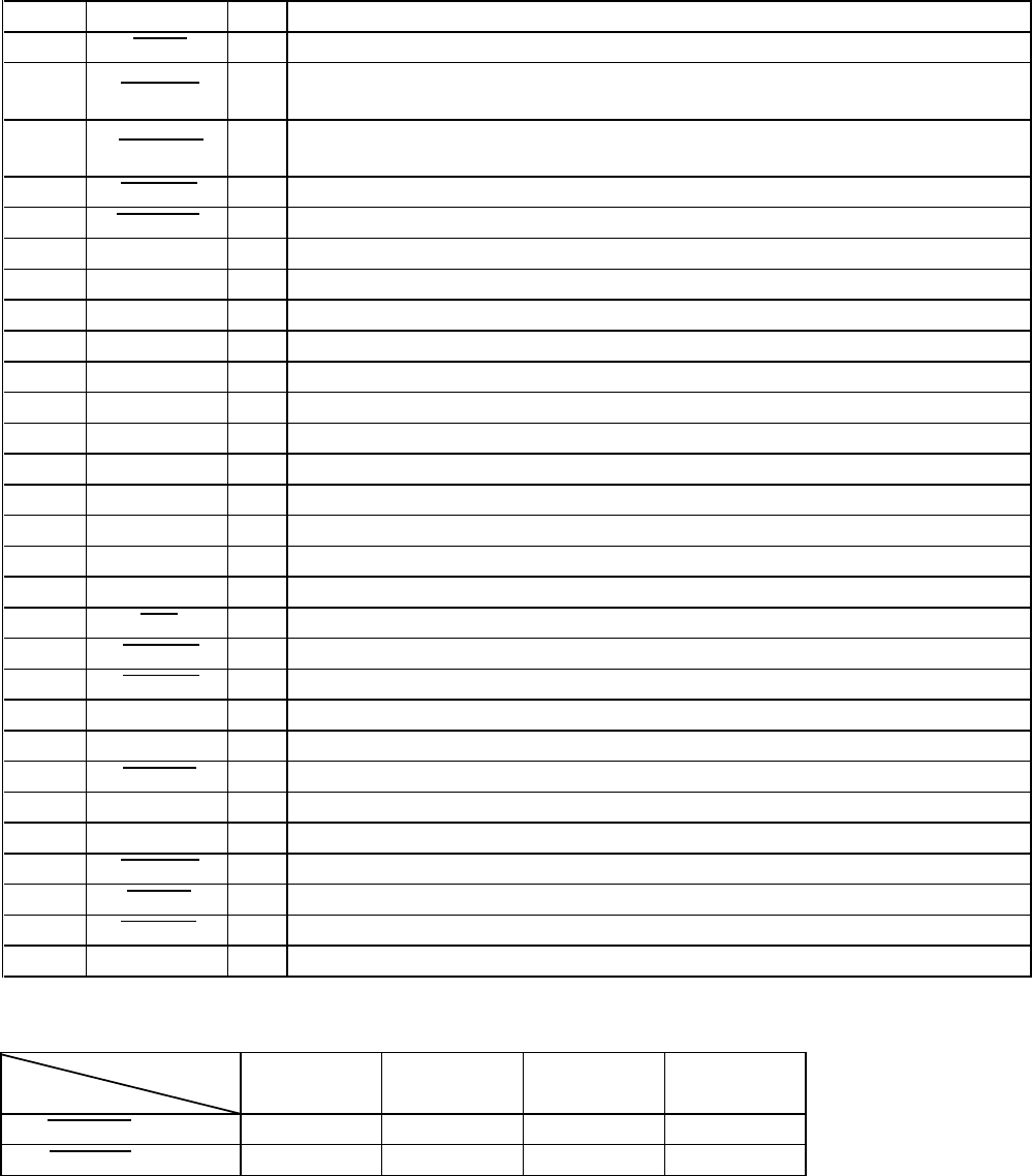
Pin No. Pin Name I/O Description
53 IN-SW I
Detection input from the tray open/close detect switch (S1) “L”: when tray is close
54 LOD POS
O
CD loading motor (M201) control signal output to the motor driver IC (IC1102)
“L” active *1
55 LOD NEG O
CD loading motor (M201) control signal output to the motor driver IC (IC1102)
“L” active *1
56 CLP POS
O Motor control signal output to the motor driver IC “L” active Not used (open)
57
CLP NEG
O
Motor control signal output to the motor driver IC “L” active Not used (open)
58 BVDD
— Power supply terminal (+5V) (for digital system)
59 BVSS
— Ground terminal (for digital system)
60 to 73
NC
O
Not used (open)
74 AVDD
— Power supply terminal (+5V)
75 AVSS
— Ground terminal
76
AVREF I Reference voltage (+5V) input terminal
77 to 80
KEY0 to KEY3 I Key input terminal (A/D input) Not used (fixed at “H”)
81 to 83
SEL0 to SEL2 I Model destination setting terminal (A/D input)
84
TEL I Tracking error level detection input terminal Not used (open)
85
SEL3 I Model (CD mechanism deck) destination setting terminal (A/D input)
86 DISC-SENS I
Detection input from the disc in detect sensor (A/D input) “H”: disc in Not used (open)
87
MECHA-JIGU
I
Not used (open)
88
ADJ I Setting terminal for the CD test mode “L”: CD test mode Normally: fixed at “H”
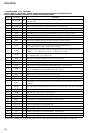
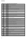
89
I2CHELP
I
Busy signal input for the IIC bus
90
I2CHELP
I
Busy signal input for the IIC bus
91
SCOR
I
Subcode sync (S0+S1) detection signal input from the CD block
92
NC O Not used (open)
93
AC-CUT
I
Power off signal input from the system controller (IC501)
94, 95
JOG0, JOG1
I
Rotary encoder jog dial pulse input terminal Not used (fixed at “L”)
96
NC O Not used (open)
97
LEDLAT O Serial data latch pulse output to a FL driver Not used
98
DRVCS
I
Chip select signal output to a FL driver Not used
99
DRVRST
I
Reset signal output to a FL driver “L”: reset Not used
100
GND — Ground terminal
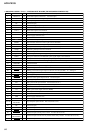
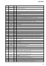
*1 Loading motor (M201) control
Mode
Terminal
LOD NEG (pin tg)
“L”“H”“L”“H”
LOD POS (pin tf)
“H”“L”“L”“H”
LOADING EJECT BRAKE RUN IDLE