


24
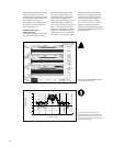
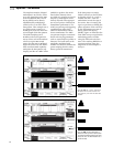
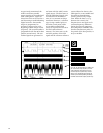
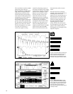
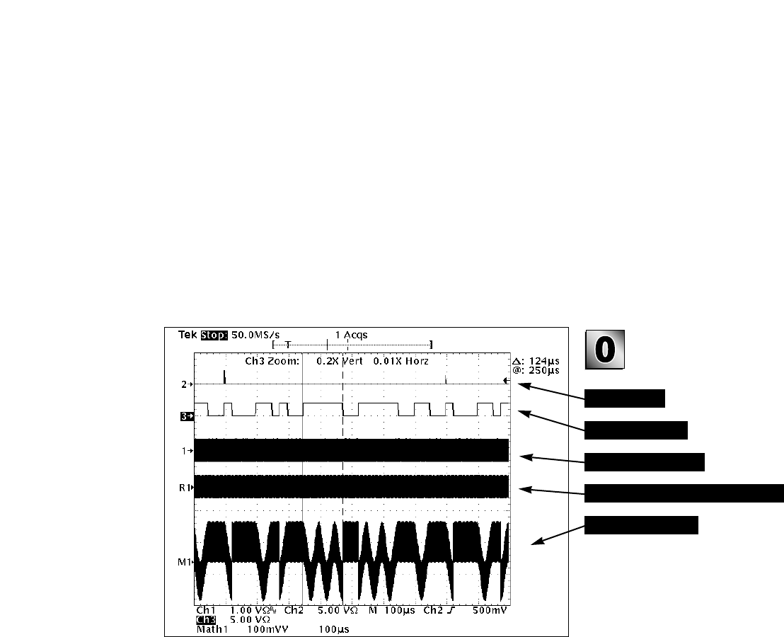
As previously mentioned, the
AWG’s two binary marker
output signals can be modulated
with a data pattern. Figure 30
shows how this can be used as a
tool for testing or troubleshooting
digital receivers. One marker
output is programmed to
generate a trigger pulse at the
beginning of each 700 µs record
(top trace). The second marker is
programmed with the 28-bit data
pattern (second trace). The two
marker signals are generated in
real time with the AWG’s main
signal output. The third trace is
the FSK modulated signal with
no indication of modulation
since it is a constant envelope
waveform. However, a coherent
copy (using a marker pulse at
the same record point) of the
10.710 MHz unmodulated
carrier is captured and saved in
the TDS 744A reference
memory. The lower trace is the
real-time product of the FSK
signal and the coherent reference
carrier. When the data is 0, the
FSK signal is at 10.710 MHz and
the coherent demodulation
yields a positive-only compo-
nent. When the data is 1 (e.g,
between the cursors), the
frequencies are not equal and a
constant frequency difference
during the interval generates a
beat component at 20 kHz. Note
that the time between peaks, or
the period of the beat product, is
50 µs or 20 kHz.
Figure 30. The TDS 744A triggers on AWG’s once
per record marker output (top trace). The TDS
744A multiplies the FSK signal by one of the
reference frequencies (lower trace). The data
pattern can be demodulated by inspection and
verified by the actual data pattern generated by
the AWG’s second marker output (second trace).
Trigger pulse
28-bit data pattern
FSK modulated signal
Reference copy of unmodulated carrier
FSK signal x carrier