


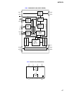
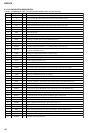
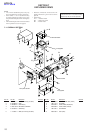
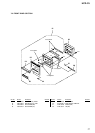
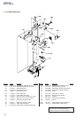
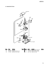

72
HCD-C5
I/OPin NamePin No. Description
—
—
—
—
—
—
—
I
I
I
O
I
O
—
I
—
I
I
I
I
—
—
O
—
I
—
—
—
I/O
I/O
O
I
O
—
—
—
—
—
—
—
—
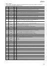
I
O
I
O
I
I
(FLDT)
(FLCK)
(LEVEL-L)
(LEVEL-R)
—
BYTE
CNVSS
XIN-T
XOUT-T
S-RST
XOUT
VSS
XIN
VCC
NMI
DQSY
P-DOWN
SQSY
(KB-CLK)
(KB-DATA)
I2C-BUSY
(A1-OUT)
XINT
(BEEP)
(XELT)
(I2C-POWER)
I2C-CLK
I2C-DAT
SWDT
SRDT
SCLK
(KB-CLK-CTL)
(CLIP-TX0)
(CLIP-RX0)
(CLIP-CLK0)
(MUTE)
(ADA-RESET)
(ADA-LATCH)
EPM
(CLIP-SEL)
—
PROTECT
EEP-CLK
CE
EEP-WP
XBUSY(MNT2)
OUT-SW
1
2
3
4
5 to 7
8
9
10
11
12
13
14
15
16
17
18
19
20
21
22
23
24
25
26
27
28
29
30
31
32
33
34
35
36
37
38
39
40
41
42
43
44
45
46
47
48
49
Not used
Not used
Not used
Not used
Not used
Data bus changed signal input (Connected to ground)
Processor mode selection terminal
Not used
Not used
System reset input
Main clock output (10MHz)
Ground
Main clock input (10MHz)
Power supply
Fixed at H (Pull-up)
Digital in sync signal input (Record system)
Power down detection signal input (L:Power down)
ADIP (MO) sync signal or subcode Q (PIT) sync signal input from the CXD2662R
(Playback system)
Not used
Not used
I2C cable connect check signal output
Not used
Interrupt status signal input from the CXD2662R
Not used
Not used
Not used
I2C serial clock input/output
I2C serial data input/output
Writing data signal output to the serial bus
Reading data signal input from the serial bus
Clock signal output to the serial bus
Not used
Not used
Not used
Not used
Not used
Not used
Not used
Not used (Pull-down)
Not used
Not used
Recording protection tab detection signal input from the protection detection switch (H:Protect)
Clock signal output to the EEP-ROM
Fixed at H (Pull-up)
Write protect signal output to the EEP ROM (L:Write enable)
Busy signal input from the CXD2662R
Detection signal input from the loading out detection switch
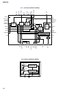
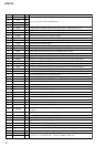
• IC701 M30803MG-A03FP MASTER CONTROLLER (MD DIGITAL BOARD)