


68
HCD-C5
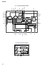
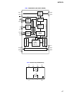
6-21. IC PIN FUNCTION DESCRIPTION
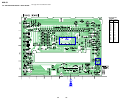
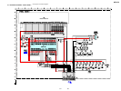
• IC101 CXA2523AR (RF AMP, FOCUS/TRACKING ERROR AMP) (BD (MD) BOARD)
I/OPin NamePin No. Description
I
I
O
I
I
—
I
O
I
I
I
I
I
O
I
O
I
I
—
I
O
I
O
O
I
I
O
O
O
O
O
O
O
I
I
O
I
I
O
I
O
I
O
I
J
VC
A to F
PD
APC
APCREF
GND
TEMPI
TEMPR
SWDT
SCLK
XLAT
XSTBY
F0CNT
VREF
EQADJ
3TADJ
VCC
WBLADJ
TE
CSLED
SE
ADFM
ADIN
ADAGC
ADFG
AUX
FE
ABCD
BOTM
PEAK
RF
RFAGC
AGCI
COMPO
COMPP
ADDC
OPO
OPN
RFO
MORFI
MORFO
1
2
3
4 to 9
10
11
12
13
14
15
16
17
18
19
20
21
22
23
24
25
26
27
28
29
30
31
32
33
34
35
36
37
38
39
40
41
42
43
44
45
46
47
48
I-V converted RF signal I input from the optical pick-up block detector
I-V converted RF signal J input from the optical pick-up block detector
Middle point voltage (+1.65V) generation output terminal
Signal input from the optical pick-up detector
Light amount monitor input from the optical pick-up block laser diode
Laser amplifier output terminal to the automatic power control circuit
Reference voltage input for setting laser power from the CXD2662R (IC151)
Ground terminal
Connected to the temperature sensor
Output terminal for a temperature sensor reference voltage
Writing serial data input from the CXD2662R (IC151)
Serial data transfer clock signal input from the CXD2662R (IC151)
Serial data latch pulse signal input from the CXD2662R (IC151)
Standby signal input terminal “L”: standby (fixed at “H” in this set)
Center frequency control voltage input terminal of internal circuit (BPF22, BPF3T, EQ) input
from the CXD2662R (IC151)
Reference voltage output terminal Not used (open)
Center frequency setting terminal for the internal circuit (EQ)
Center frequency setting terminal for the internal circuit (BPF3T)
Power supply terminal (+3.3V)
Center frequency setting terminal for the internal circuit (BPF22)
Tracking error signal output to the CXD2662R (IC151)
Connected to the external capacitor for low-pass filter of the sled error signal
Sled error signal output to the CXD2662R (IC151)
FM signal output of the ADIP
Receives a ADIP FM signal in AC coupling
Connected to the external capacitor for ADIP AGC
ADIP duplex signal (22.05 kHz ± 1 kHz) output to the CXD2662R (IC151)
Auxiliary signal (I3 signal/temperature signal) output to the CXD2662R (IC151)
Focus error signal output to the CXD2662R (IC151)
Light amount signal (ABCD) output to the CXD2662R (IC151)
Light amount signal (RF/ABCD) bottom hold output to the CXD2662R (IC151)
Light amount signal (RF/ABCD) peak hold output to the CXD2662R (IC151)
Playback EFM RF signal output to the CXD2662R (IC151)
Connected to the external capacitor for RF auto gain control circuit
Receives a RF signal in AC coupling
User comparator output terminal Not used (open)
User comparator input terminal Not used (fixed at “L”)
Connected to the external capacitor for cutting the low band of the ADIP amplifier
User operational amplifier output terminal Not used (open)
User operational amplifier inversion input terminal Not used (fixed at “L”)
RF signal output terminal
Receives a MO RF signal in AC coupling
MO RF signal output terminal