


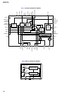
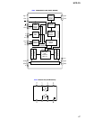

70
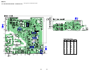
HCD-C5
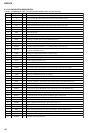
I/OPin NamePin No. Description
I/O
I/O
I/O
I/O
I (S)
O
I (A)
—
I (A)
I (A)
—
O (3)
I (A)
O (A)
I (A)
I (A)
I (A)
I (A)
I (A)
I (A)
I (A)
O (A)
—
I (A)
I (A)
—
I (A)
I (A)
I (A)
I
I (S)
O
O
O
O
O
O
O
O
—
O
O
O
O
O
O
D1
D0
D2
D3
MVCI
ASYO
ASYI
AVDD
BIAS
RFI
AVSS
PCO
FILI
FILO
CLTV
PEAK
BOTM
ABCD
FE
AUX1
VC
ADIO
AVDD
ADRT
ADRB
AVSS
SE
TE
DCHG
TEST4
ADFG
F0CNT
XLRF
CKRF
DTRF
APCREF
TEST0
TRDR
TFDR
DVDD
FFDR
FRDR
FS4
SRDR
SFDR
SPRD
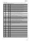
48
49
50
51
52
53
54
55
56
57
58
59
60
61
62
63
64
65
66
67
68
69
70
71
72
73
74
75
76
77
78
79
80
81
82
83
84
85
86
87
88
89
90
91
92
93
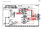
Two-way data bus with the D-RAM (IC152)
Digital in PLL oscillation input from the external VCO Not used (fixed at “L”)
Playback EFM full-swing output terminal
Playback EFM asymmetry comparator voltage input terminal
Power supply terminal (+3.3V) (analog system)
Playback EFM asymmetry circuit constant current input terminal
Playback EFM RF signal input from the CXA2523AR (IC101)
Ground terminal (analog system)
Phase comparison output for master clock of the recording/playback EFM master PLL
Filter input for master clock of the recording/playback master PLL
Filter output for master clock of the recording/playback master PLL
Internal VCO control voltage input of the recording/playback master PLL
Light amount signal (RF/ABCD) peak hold input from the CXA2523AR (IC101)
Light amount signal (RF/ABCD) bottom hold input from the CXA2523AR (IC101)
Light amount signal (ABCD) input from the CXA2523AR (IC101)
Focus error signal input from the CXA2523AR (IC101)
Auxiliary signal (I3 signal/temperature signal) input from the CXA2523AR (IC101)
Middle point voltage (+1.65V) input from the CXA2523AR (IC101)
Monitor output of the A/D converter input signal Not used (open)
Power supply terminal (+3.3V) (analog system)
A/D converter operational range upper limit voltage input terminal (fixed at “H” in this set)
A/D converter operational range lower limit voltage input terminal (fixed at “L” in this set)
Ground terminal (analog system)
Sled error signal input from the CXA2523AR (IC101)
Tracking error signal input from the CXA2523AR (IC101)
Connected to the +3.3V power supply
nput terminal for the test Not used (fixed at “H”)
ADIP duplex FM signal (22.05 kHz ± 1 kHz) input from the CXA2523AR (IC101)
Filter f0 control signal output to the CXA2523AR (IC101)
Serial data latch pulse signal output to the CXA2523AR (IC101)
Serial data transfer clock signal output to the CXA2523AR (IC101)
Writing serial data output to the CXA2523AR (IC101)
Control signal output to the reference voltage generator circuit for the laser automatic power
control
Input terminal for the test Not used (open)
Tracking servo drive PWM signal (–) output to the BH6511FS (IC141)
Tracking servo drive PWM signal (+) output to the BH6511FS (IC141)
Power supply terminal (+3.3V) (digital system)
Focus servo drive PWM signal (+) output to the BH6511FS (IC141)
Focus servo drive PWM signal (–) output to the BH6511FS (IC141)
Clock signal (176.4 kHz) output terminal (X’tal system) Not used (open)
Sled servo drive PWM signal (–) output to the BH6511FS (IC141)
Sled servo drive PWM signal (+) output to the BH6511FS (IC141)
Spindle servo drive PWM signal (–) output to the BH6511FS (IC141)
* I (S) stands for schmitt input, I (A) for analog input, O (3) for 3-state output, and O (A) for analog output in the column I/O.