ADCSOCAO
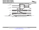
or
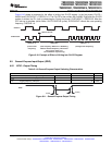
ADCSOCBO
t
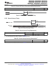
w(ADCSOCAL)
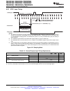
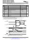
XNMI, XINT1, XINT2
t
w(INT)
Interrupt Vector
t
d(INT)
Address bus
(internal)
TMS320F2809, TMS320F2808, TMS320F2806
TMS320F2802, TMS320F2801, TMS320C2802
TMS320C2801, TMS320F28016, TMS320F28015
www.ti.com
SPRS230L–OCTOBER 2003–REVISED DECEMBER 2009
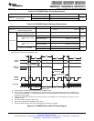
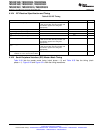
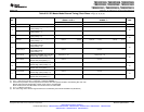
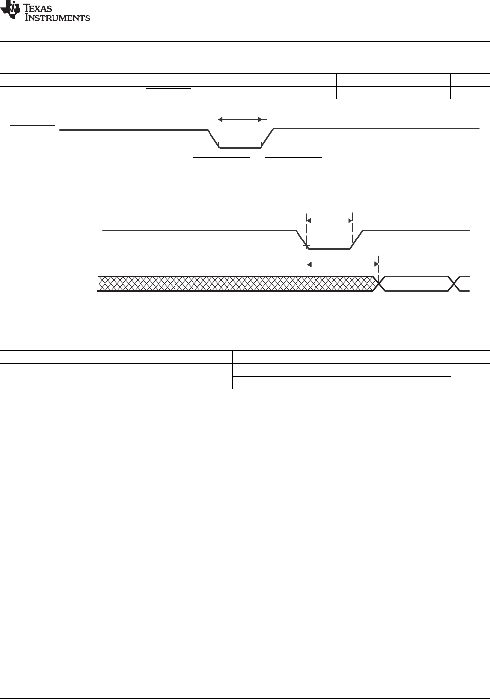
Table 6-30. External ADC Start-of-Conversion Switching Characteristics
PARAMETER MIN MAX UNIT
t
w(ADCSOCAL)
Pulse duration, ADCSOCAO low 32t
c(HCO )
cycles
Figure 6-18. ADCSOCAO or ADCSOCBO Timing
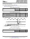
6.10.3 External Interrupt Timing
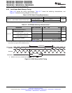
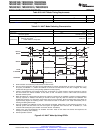
Figure 6-19. External Interrupt Timing
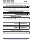
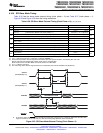
Table 6-31. External Interrupt Timing Requirements
(1)
TEST CONDITIONS MIN MAX UNIT
t
w(INT)
(2)
Pulse duration, INT input low/high Synchronous 1t
c(SCO)
cycles
With qualifier 1t
c(SCO)
+ t
w(IQSW)
(1) For an explanation of the input qualifier parameters, see Table 6-15 .
(2) This timing is applicable to any GPIO pin configured for ADCSOC functionality.
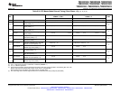
Table 6-32. External Interrupt Switching Characteristics
(1)
PARAMETER MIN MAX UNIT
t
d(INT)
Delay time, INT low/high to interrupt-vector fetch t
w(IQSW)
+ 12t
c(SCO)
cycles
(1) For an explanation of the input qualifier parameters, see Table 6-15 .
Copyright © 2003–2009, Texas Instruments Incorporated Electrical Specifications 117
Submit Documentation Feedback
Product Folder Link(s): TMS320F2809 TMS320F2808 TMS320F2806 TMS320F2802 TMS320F2801 TMS320C2802
TMS320C2801 TMS320F28016 TMS320F28015


