


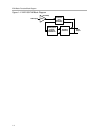

EVM Basic Function/Block Diagram
1-3
EVM Overview
and NPN transistor circuit is used to create the 3-V supply for the TPA2001D1
and TLV2464A; therefore, the user only needs to apply the single-supply
voltage. A+ supply is used for powering the TAS5111 and is input for the zener
diode/NPN transistor circuit used to generate the 3-V supply for the
TPA2001D1 and TLV2464A.
To avoid potential damage to the EVM board, make sure that the
correct cables are connected to their respective terminals as
labeled on the EVM board.
Stresses above 29.5-V maximum voltage rating may cause
permanent damage to the TAS5111.
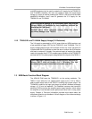
1.2.2 TPA2001D1 and TLV2464A Supply Voltage (3-V Reference)
The 3-V supply is generated by a 3.9-V zener diode, an NPN transistor, and
a few resistors to supply VDD for the TPA2001D1 and TLV2464A. The 3-V
supply voltage goes through a 20-Ω resistor to filter any noise. Test point 3V
is placed after the 20-Ω resistor to allow the user to remove the 20-Ω resistor
and insert an external 3-V supply. If an external supply is inserted, the voltage
needs to be greater than 2.75 V to enable proper operation of the TPA2001D1
and less than 3.6 V to allow proper voltage levels to the inputs of the TAS5111.
When applying an external voltage reference through test point 3V,
ensure that it does not exceed +3.6 V. Otherwise, this can
permanently damage the installed device under test (DUT).
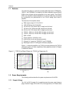
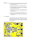
1.3 EVM Basic Function/Block Diagram
The APA100 EVM uses the TPA2001D1 as the analog modulator. The
TAS5111 level shifts the 3-V, peak-to-peak output to the 18-V to 29.5-V,
peak-to-peak output level of the TAS5111 enabling high−power output. The
TLV2464A is used for the input gain stage, to provide a buffered midsupply
voltage (1.5 V) and as feedback. The feedback improves total harmonic
distortion (THD) and gives the amplifier power supply rejection, which allows
the amplifier to have excellent audio performance even with a noisy power
supply. Chapter 4, Technical Information provides more details about the
component selection and feedback. A block diagram of the reference design
is shown in Figure 1−2.