


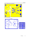

PCB Layout
2-3
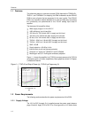
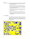
PCB Design
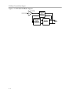
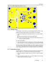
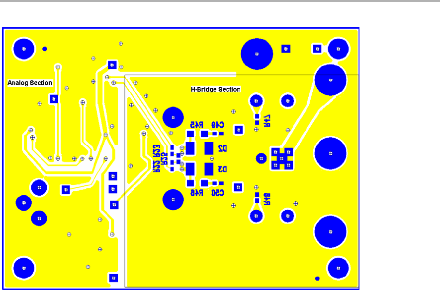
Figure 2−2. APA100 Split Plane Bottom Layout
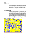
2.1.2 H-Bridge Layout
The H-bridge is laid out based on recommendations from the TAS5111 data
sheet and follows the same pattern as the DAVREF100 EVM board.
1) Keep local decoupling and bootstrap capacitors and resistors close to
pins.
J Minimize trace length to C29, and use wide traces.
J Local PVDD decoupling R35, C35, R36, and C36 traces should be as
short and as wide as possible.
2) Use a ground plane.
3) Use trace impedance from bulk decoupling to PVDD pin, making the trace
50 mm long and 1 mm wide, with separate traces for PVDDA and PVDDB
To ensure proper H-bridge layout, measure the TAS5111 output waveforms at
the pins with a short ground lead on the scope probe to PGND. See application
report Voltage Spike Measurement Technique and Specification (SLEA025).
2.1.3 Analog Section Layout
The analog section is carefully laid out to keep the switching currents from the
TAS5111 away from it. The EVM layout followed these general rules.
1) Keep the operational amplifier away from TAS5111 output and power
traces.
2) Minimize nodes connected to IN− pin of the TLV2464A. This is the most
sensitive node of the reference design.