


PCB Layout
2-2
2.1 PCB Layout
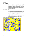
The critical part of the design lies particularly in the layout process. The EVM
layout should be followed exactly for optimal performance. The main concern
is the placement of components and the proper routing of signals. Place the
bypass/decoupling capacitors as close as possible to the pins; properly
separate the linear and switching signals from each other. Because of its
importance, carefully consider the ground plane in the layout process. A split
ground plane is ideally preferred.
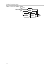
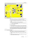
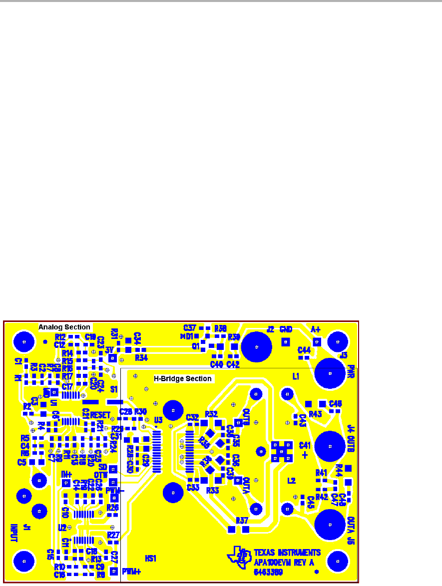
2.1.1 Split Ground Plane
The split plane used in the EVM separates the ground plane for the H−bridge
and a separate plane for everything else. The ground plane plays an important
role in controlling the noise and other effects that contribute to distortion and
noise on the output. To ensure that the return currents are handled properly,
route the appropriate signals only in their respective sections; this means that
the analog traces should only lay directly above or below the analog ground
section and the H-bridge traces in the H-bridge ground section. Minimize the
length of the traces. Figure 2−1 shows the top layer labeled with Analog
Section and H-Bridge Section to demonstrate how the board is split. The
bottom layer is split along the same line, as shown in Figure 2−2.
Figure 2−1. APA100 Split Plane Top Layout