


47
MZ-B10
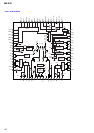
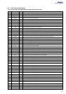
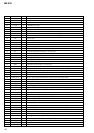
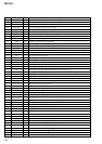
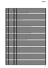
6-9. IC Pin Function Description
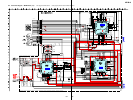
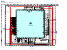
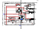
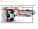
• IC801 CXD2680-207GA (SYSTEM CONTROLLER, DIGITAL SIGNAL PROCESSOR)
Pin No.
1
2
3
4
5
6
7
8
9
10
11
12
13
14
15
16
17
18
19
20
21
22
23
24
25
26
27
28
29
30
31
32
33
34
35
36
37
38
39
40
41
42
43
44
45
46
47
48
49
50
I/O
I
O
O
O
O
O
O
I
I
I
O
I
O
I
I
I
I
I
I
O
I
I
I
I
I
I
I
I
O
O
O
O
O
O
O
O
O
O
O
I
I
I
O
O
I
I
I
O
I
O
Pin Name
OSCI
OSCO
VREFL
AOUTL
AOUTR
VREFR
ASYO
ASYI
BIAS
RFI
PCO
FILI
FILO
CLTV
PEAK
BOTM
ABCD
FE
VC
ADIO
ADRB
SE
TE
AUX1
ADRT
DCHG
APC
ADFG
APCREF
TRDR
TFDR
FFDR
FRDR
FS4
SFDR
SPRD
SPFD
SPDV
SPDW
SPCU
SPCV
SPCW
SLDV
SLDW
SLCU
SLCV
SLCW
SRDR
DIN
DADT
Description
Resonator connection terminal for the system clock (22.5792MHz)
Resonator connection terminal for the system clock (22.5792MHz)
Reference voltage terminal connected to the capacitor (for the built-in D/A converter L-CH)
Built-in D/A converter L-CH signal output
Built-in D/A converter R-CH signal output
Reference voltage terminal connected to the capacitor (for the built-in D/A converter R-CH)
Playback EFM duplex signal output
Playback EFM comparator slice level input
Bias current input terminal for the playback EFM comparator
Playback EFM RF signal input from the RF amplifier
Phase comparison output terminal for the playback EFM system master PLL
Filter input terminal for the playback EFM system master PLL
Filter output terminal for the playback EFM system master PLL
Internal VCO control voltage input terminal for the playback EFM system master PLL
Peak hold signal input of the light amount signal (RF/ABCD) from the RF amplifier
Bottom hold signal input of the light amount signal (RF/ABCD) from the RF amplifier
Light amount signal (ABCD) input from the RF amplifier
Focus error signal input from the RF amplifier
Middle point voltage input from the RF amplifier
Monitor output terminal of A/D converter input signal Not used (open)
The lower limit voltage of A/D converter input terminal (connected to the ground)
Sled error signal input from the RF amplifier
Tracking error signal input from the RF amplifier
Auxiliary A/D input (fixed at “H” in this set)
The upper limit voltage of A/D converter input terminal (fixed at “H” in this set)
Connecting terminal with the analog power supply of low impedance (fixed at “H” in this set)
Error signal input for the laser automatic power control (fixed at “H” in this set)
ADIP duplex FM signal (22.05±1kHz) input from the RF amplifier
Reference PWM signal output for the laser automatic power control to the RF amplifier
Tracking servo drive PWM signal output (–) to the coil driver
Tracking servo drive PWM signal output (+) to the coil driver
Focus servo drive PWM signal output (+) to the coil driver
Focus servo drive PWM signal output (–) to the coil driver
176.4kHz clock signal output
Sled servo drive PWM signal output to the motor driver
Spindle motor drive control signal output (U) to the motor driver
Spindle servo drive PWM signal output to the motor driver
Spindle motor drive control signal output (V) to the motor driver
Spindle motor drive control signal output (W) to the motor driver
Spindle motor drive comparison signal input (U) from the motor driver
Spindle motor drive comparison signal input (V) from the motor driver
Spindle motor drive comparison signal input (W) from the motor driver
Sled motor drive control signal output (V) to the motor driver
Sled motor drive control signal output (W) to the motor driver
Sled motor drive comparison signal input (U) from the motor driver
Sled motor drive comparison signal input (V) from the motor driver
Sled motor drive comparison signal input (W) from the motor driver
Sled motor drive control signal output (U) to the motor driver
Digital audio signal input
Audio data output terminal Not used (open)
Ver 1.2 2003.09