


YMF715E
May 21, 1997
-45-
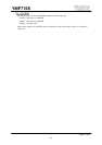
Note : DV
SS
=AV
SS
=0[V], T
OP
=0~70 , AV
DD
=5.0[V]
*1 : Applicable to s
chmitt
input pins without /VOLUP, /VOLDW.
*2 : Applicable to /VOLUP and /VOLDW pins.
*3 : When V
OL1
=max. 0.5V, the value into the brackets is specified at I
OHL1, 2
.
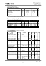
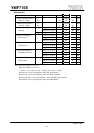
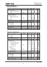
DC Characteristics 2
(DV
DD
= 3.3 0.30[V])
Note : DV
SS
=AV
SS
=0[V], T
OP
=0~70 , AV
DD
=5.0[V]
The specifications marked “*” are different from the value at DV
DD
= 5.0 0.25[V].
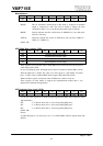
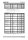
Item Symbol Condition Min. Typ. Max. Unit
CMOS Output pins
High Level Output Voltage 2
V
OH2
I
OH
=2mA 0.8DV
DD
V
Low Level Output Voltage 2
V
OL2
I
OL
=2mA 0.4 V
Output Leakage Current O
L
Hi_Z:V
IN
=DV
SS
, DV
DD
-10 10 A
Output Capacitance C
O
10 pF
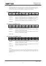
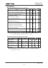
Item Symbol Condition Min. Typ. Max. Unit
TTL-Input Pins
High Level Input Voltage 1
V
IH1
Except 2.0 V
Low Level Input Voltage 1
V
IL1
schmitt inputs 0.8 V
CMOS-Input Pins
High Level Input Voltage 2
V
IH2
0.7DV
DD
V
Low Level Input Voltage 2
V
IL2
0.2DV
DD
V
Schmitt Vt- (H to L) V
t
-0.81.5V
Schmitt Vt+ (L to H) V
t
+ 1.3 2.2 * V
Schmitt Hysteresis V
h
0.3 * V
Input Leakage Current I
L
V
IN
=DV
SS
, DV
DD
-10 10 A
Input Capacitance C
I
10 pF
R
U1
RXD 20 50 100 k
Pull up Register R
U2
GP7 ~ 4 30 100 200 k
R
U3
Otherwise 50 200 400 k
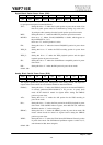
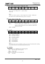
TTL-Output Pins
High Level Output Voltage 1
V
OH1
2.4 V
Low Level Output Voltage 1
V
OL1
0.4 V
TTL Output Current I
OHL1
D7 ~ 0 pins 2 * mA
I
OHL2
IRQn, DRQn pins 2 * mA
I
OHL3
TXD pin 2 * mA
I
OHL4
MP9 ~ 0 pins 2 mA
CMOS Output pins
High Level Output Voltage 2
V
OH2
I
OH
=2mA 0.8DV
DD
V
Low Level Output Voltage 2
V
OL2
I
OL
=2mA 0.4 V
Output Leakage Current O
L
Hi_Z:V
IN
=DV
SS
, DV
DD
-10 10 A
Output Capacitance C
O
10 pF