


TMS320F2809, TMS320F2808, TMS320F2806
TMS320F2802, TMS320F2801, TMS320C2802
TMS320C2801, TMS320F28016, TMS320F28015
www.ti.com
SPRS230L–OCTOBER 2003–REVISED DECEMBER 2009
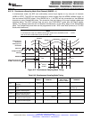
6.10.7 On-Chip Analog-to-Digital Converter
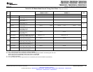
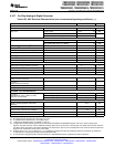
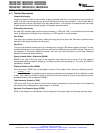
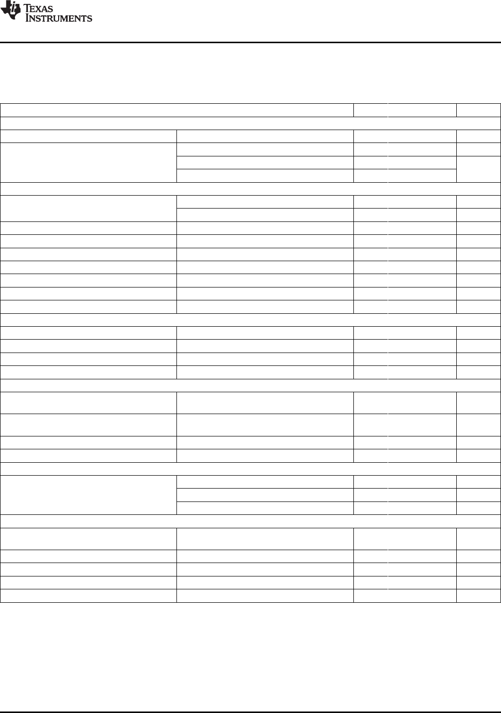
Table 6-38. ADC Electrical Characteristics (over recommended operating conditions)
(1) (2)
PARAMETER MIN TYP MAX UNIT
DC SPECIFICATIONS
Resolution 12 Bits
ADC clock 60-MHz device 0.001 7.5 MHz
100-MHz device 0.001 12.5 MHz
100-MHz device (F2809 only) 0.001 25
ACCURACY
INL (Integral nonlinearity) 1–12.5 MHz ADC clock (6.25 MSPS) ±1.5 LSB
12.5–25 MHz ADC clock (12.5 MSPS) ±2 LSB
DNL (Differential nonlinearity)
(3)
±1 LSB
Offset error
(4)
–60 +60 LSB
Offset error with hardware trimming ±4 LSB
Overall gain error with internal reference
(5)
–60 +60 LSB
Overall gain error with external reference –60 +60 LSB
Channel-to-channel offset variation ±4 LSB
Channel-to-channel gain variation ±4 LSB
ANALOG INPUT
Analog input voltage (ADCINx to ADCLO)
(6)
0 3 V
ADCLO –5 0 5 mV
Input capacitance 10 pF
Input leakage current ±5 μA
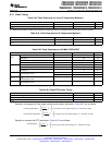
INTERNAL VOLTAGE REFERENCE
(5)
V
ADCREFP
- ADCREFP output voltage at the pin 1.275 V
based on internal reference
V
ADCREFM
- ADCREFM output voltage at the pin 0.525 V
based on internal reference
Voltage difference, ADCREFP - ADCREFM 0.75 V
Temperature coefficient 50 PPM/°C
EXTERNAL VOLTAGE REFERENCE
(5) (7)
ADCREFSEL[15:14] = 11b 1.024 V
V
ADCREFIN
- External reference voltage input on
ADCREFIN pin 0.2% or better accurate ADCREFSEL[15:14] = 10b 1.500 V
reference recommended
ADCREFSEL[15:14] = 01b 2.048 V
AC SPECIFICATIONS
SINAD (100 kHz) Signal-to-noise ratio + 67.5 dB
distortion
SNR (100 kHz) Signal-to-noise ratio 68 dB
THD (100 kHz) Total harmonic distortion –79 dB
ENOB (100 kHz) Effective number of bits 10.9 Bits
SFDR (100 kHz) Spurious free dynamic range 83 dB
(1) Tested at 12.5 MHz ADCCLK.
(2) All voltages listed in this table are with respect to V
SSA2
.
(3) TI specifies that the ADC will have no missing codes.
(4) 1 LSB has the weighted value of 3.0/4096 = 0.732 mV.
(5) A single internal/external band gap reference sources both ADCREFP and ADCREFM signals, and hence, these voltages track
together. The ADC converter uses the difference between these two as its reference. The total gain error listed for the internal reference
is inclusive of the movement of the internal bandgap over temperature. Gain error over temperature for the external reference option will
depend on the temperature profile of the source used.
(6) Voltages above V
DDA
+ 0.3 V or below V
SS
- 0.3 V applied to an analog input pin may temporarily affect the conversion of another pin.
To avoid this, the analog inputs should be kept within these limits.
(7) TI recommends using high precision external reference TI part REF3020/3120 or equivalent for 2.048-V reference.
Copyright © 2003–2009, Texas Instruments Incorporated Electrical Specifications 125
Submit Documentation Feedback
Product Folder Link(s): TMS320F2809 TMS320F2808 TMS320F2806 TMS320F2802 TMS320F2801 TMS320C2802
TMS320C2801 TMS320F28016 TMS320F28015