


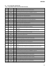

37
MZ-R900
Pin No.
Pin Name
I/O Description
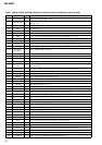
156, 157 TEST1, TEST0 I Input terminal for the main test (normally fixed at “L”)
158 EVA I EVA/FLASH chip discrimination terminal “L”: FLASH chip, “H”: EVA chip
159 NC O Not used (open)
160 SSB DATA I/O Input/output of SSB serial data with RF amp (IC501)
161 SSB CLK O SSB serial clock output to RF amp (IC501)
162 MCUVSS0
—
Ground terminal (for the microcomputer block)
163 VREC PWM O Over write head control spare terminal Not used (open)
164 VL PWM I
PWM for the laser automatic power supply voltage control signal output to the power control
(IC901)
165 VC PWM I PWM signal output for the system power supply voltage control to the power control (IC901)
166
SPDL AUX
PWM
O PWM signal output for the spindle support to the motor driver (IC551)
167, 168 NC O Not used (open)
169 CLK SEL O System clock select signal output to the power control (IC901)
170
OPEN CLOSE
SW
I
Open/close detection switch (S806) of the upper panel input terminal (A/D input)
“L”: when upper panel close
171 GND SW O Control signal output to the ground (GND) changeover switch
172 SET CODE0 O Input terminal for the set (fixed at “L” except for US/Canadian)
173 SET CODE1 O Input terminal for the set (open in this set)
174, 175 SET CODE2, 3 O Input terminal for the set (fixed at “L” in this set)
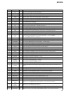
176 MIFVDD1
—
Power supply terminal (for the microcomputer I/F block) (+2.3V)
177 MIFVSS1
—
Ground terminal (for the microcomputer I/F block)
178 AOUT SEL O HP/LINE changeover signal output to the headphone amp (IC302)
179 SI0 I
Serial data input from the nonvolatile memory (IC804) and liquid crystal display element
module
180 SO0 O
Serial data output to the nonvolatile memory (IC804), A/D, D/A converter (IC301) and
liquid crystal display element module
181 SCK0 O
Serial clock signal output to the nonvolatile memory (IC804), A/D, D/A converter (IC301)
and liquid crystal display element module
182 XGUM ON I
Battery pack detection switch (S804) input terminal for the charge “L”: there is battery pack
for the charge
183 BEEP O Beep sound control signal output to the headphone amp (IC302)
184 NC O Not used (open)
185 VD SEL O VD power supply changeover signal output terminal Not used (open)
186 XMUTE O
Analog muting control signal output terminal to the headphone amp (IC302)
“L”: muting ON
187 LCD RST AUX O Reset control signal output terminal to the liquid crystal display element “L”: reset
188, 189 NC O Not used (open)
190 XPATCH I Patch function detection input terminal “L”: patch function Not used (open)
191 OPT DET I DIN plug detection signal input terminal
192 XJACK DET I LINE IN plug detection signal input terminal
193 XMIC DET I Microphone plug detection signal input terminal
194, 195 PD S0, PD S1 O PD IC mode changeover signal output to the optical pick up
196 MIFVDD2
—
Power supply terminal (for the microcomputer I/F block) (+2.3V)
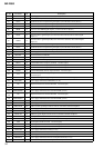
197 to
199
MODE1 to 3 O
Power supply control signal output (for the over write head drive) to the over write head
drive (IC601)
200, 201 HD CON 1, 2 O Over write head control signal output to the over write head drive (IC601)
202 REC WBL SW O LPF changeover switch input terminal when REC/PB control Not used (open)
203 XCS ADA O Chip select signal output to A/D, D/A converter (IC301)