


Applications Engineering
Appendix C. Expansion Headers
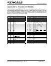
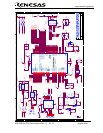
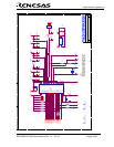
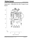
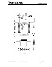
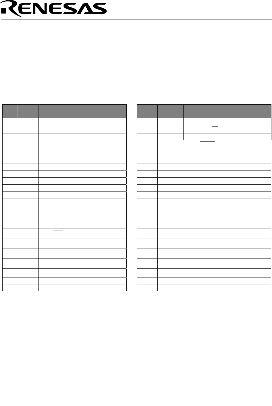
The M30280FA MCU on the RZB-ZMD16C-ZDK target board is housed in an 80-pin QFP package. Pin 1
of the package is identified by a little white circle on the board’s top silkscreen. Connectors J1 to J4,
located around the MCU, provide access to almost all of the MCU’s pins. You can use J1-J4 as test
points to check MCU signals or, by mounting your own headers, connect your own expansion board. The
silkscreen identifying the connectors is at the bottom of the ZDK board. The following table shows the
mapping of J1-J4 pins to MCU pins and signal names.
J1
Pin
MCU
Pin
MCU Function
J2
Pin
MCU
Pin
MCU Function
1 1 P9
5
/AN
25
/CLK
4
1 21 P7
6
/TA
3out
2 2 P9
3
/AN
24
2 22
P7
5
/TA
2in
/ W
3 3 P9
2
/TB
2in
3 23 P7
4
/TA
2out
/W
4 4 P9
1
/TB
1in
4 24
P7
3
/
2
CTS /
2
RTS /TA
1in
/ V
/TXD
1
5 5 P9
0
/TB
0in
5 25 P7
2
/CLK
2
/TA
1out
/V/RXD
1
6 6 26 P7
1
/RxD
2
/SCL/TA
0in
/CLK
1
7 7 27 P7
0
/TxD
2
/SDA/TA
0out
8 8 28 P6
7
/TxD
1
9 9 29 P6
6
/RxD
1
10 10 30 P6
5
/CLK
1
11 11 Vss 11 31
P6
4
/
1
CTS /
1
RTS /
0
CTS
/CLKS
1
12 12 32 P3
7
13 13 Vcc 13 33 P3
6
14 14
P8
5
/NMI/ SD
14 34 P3
5
15 15
P8
4
/
2
INT /Zphase
15 35 P3
4
16 16
P8
3
/
1
INT
16 36 P3
3
17 17
P8
2
/
0
INT
17 37 P3
2
/S
OUT3
18 18
P8
1
/TA
4in
/U
18 38 P3
1
/S
IN3
19 19 P8
0
/TA
4out
/U 19 39 P3
0
/CLK
3
20 20 P7
7
/TA
3in
20 40 P6
3
/TxD
0
RZB-ZMD16C-ZDK User’s Manual Rev 1.2 26/ 33 August 2006