


Applications Engineering
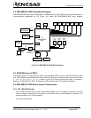
5.4.2. JP2: Power LED (D4) and RS232 (U7) Transceiver Power
JP2 is used to connect the Vcc pin of the RS232 transceiver chip (U7) to the 3.3V supply of the board.
It also connects the red Power LED (D4) to the board’s supply. It can be used to reduce the board’s
power consumption by disconnecting the RS232 transceiver and Power LED. For normal operations,
JP2 must be shorted.
JP2 is shorted by default.
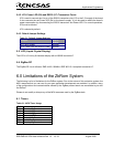
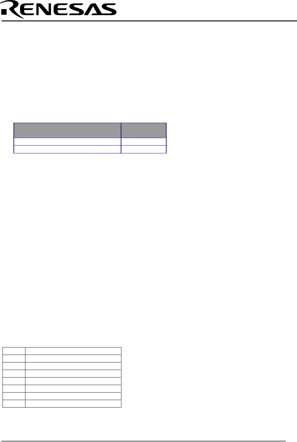
5.4.3. Default Jumper Settings
Table 5-1: Default Jumper Settings
Jumper Default
Setting
JP1: MCU Power Shorted
JP2: Power LED and RS232 Power Shorted
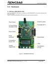
5.5. LCD (Liquid Crystal Display)
The LCD is a 2-line by 8-character display with a KS0066 controller IC.
5.6. ZigBee RF
The ZigBee RF circuit utilizes a ZMD 44102, 900MHz, IEEE 802.15.4 compliant transceiver IC.
6.0 Limitations of the ZbRom System
The following is a list of limitations for the ZbRom system. Due to the nature of this evaluation system, the
MCU resources that you can use for your own application development are restricted. In addition, many
of the configurations and customizations offered by the ZigBee protocol stack are unavailable to you with
the ZbRom.
Please do not modify or disrupt any of the MCU resources used by the ZigBee stack:
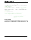
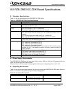
6.1. Timers
Table 6-1: MCU Timer Usage
TA0 available
TA1 Used by ZigBee stack
TA2 Used by ZigBee stack
TA3 Used by ZigBee stack
TA4 Used by RTOS
TB0 Used by ZigBee stack
TB1 available
TB2 Used by ZigBee stack
RZB-ZMD16C-ZDK User’s Manual Rev 1.2 13/ 33 August 2006