


Philips Semiconductors Product data sheet
SC28L91
3.3 V or 5.0 V Universal Asynchronous
Receiver/Transmitter (UART)
2004 Oct 21
9
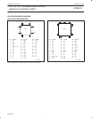
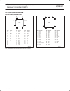
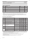
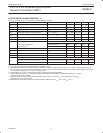
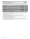
PIN CONFIGURATION FOR 68XXX BUS INTERFACE (MOTOROLA
)
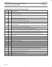
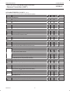
Symbol
Pin
type
Name and function
I/M I Bus Configuration: When low configures the bus interface to the Conditions shown in this table.
D0–D7 I/O Data Bus: Bi-directional 3-State data bus used to transfer commands, data and status between the UART and the
CPU. D0 is the least significant bit.
CEN I Chip Enable: Active-Low input signal. When Low, data transfers between the CPU and the UART are enabled on
D0–D7 as controlled by the R/WN and A0–A3 inputs. When High, places the D0–D7 lines in the 3-State condition.
R/WN I Read/Write: Input Signal. When CEN is low R/WN high input indicates a read cycle; when low indicates a write cycle.
IACKN I Interrupt Acknowledge: Active low input indicating an interrupt acknowledge cycle. Usually asserted by the CPU in
response to an interrupt request. When asserted places the interrupt vector on the bus and asserts DACKN.
DACKN O Data Transfer Acknowledge: A3-State active-low output asserted in a write, read, or interrupt acknowledge cycle to
indicate proper transfer of data between the CPU and the UART.
A0–A3 I Address Inputs: Select the UART internal registers and ports for read/write operations.
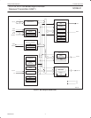
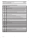
RESETN I Reset: A low level clears internal registers (SRA, SRB, IMR, ISR, OPR, OPCR), puts OP0–OP7 in the High state,
stops the counter/timer, and puts the Channel in the inactive state, with the TxD outputs in the mark (High) state. Sets
MR pointer to MR1. See Figure 4
INTRN O Interrupt Request: Active-Low, open-drain, output which signals the CPU that one or more of the eight maskable
interrupting conditions are true. This pin requires a pullup.
X1/CLK I Crystal 1: Crystal or external clock input. A crystal or clock of the specified limits must be supplied at all times. When
a crystal is used, a capacitor must be connected from this pin to ground (see Figure 11).
X2 O Crystal 2: Connection for other side of the crystal. When a crystal is used, a capacitor must be connected from this
pin to ground (see Figure 11). If X1/CLK is driven from an external source, this pin must be left open.
RxD I Receiver Serial Data Input: The least significant bit is received first. “Mark” is High, “space” is Low.
TxD O Transmitter Serial Data Output: The least significant bit is transmitted first. This output is held in the ‘mark’ condition
when the transmitter is disabled, idle, or when operating in local loop back mode. ‘Mark’ is High; ‘space’ is Low.
OP0 O Output 0: General purpose output or request to send (RTSAN, active-Low). Can be deactivated automatically on
receive or transmit.
OP1 O Output 1: General-purpose output.
OP2 O Output 2: General purpose output or transmitter 1X or 16X clock output, or receiver 1X clock output.
OP3 O Output 3: General purpose output.
OP4 O Output 4: General purpose output or open-drain, active-Low, RxA interrupt ISR [1] output. DMA Control
OP5 O Output 5: General-purpose output.
OP6 O Output 6: General purpose output or open-drain, active-Low, TxA interrupt ISR[0] output. DMA Control
OP7 O Output 7: General-purpose output.
IP0 I Input 0: General purpose input or clear to send active-Low input (CTSAN). Has Change of State Dector.
IP1 I Input 1: General purpose input. Has Change of State Dector.
IP2 I Input 2: General-purpose input or counter/timer external clock input. Has Change of State Dector.
IP3 I Input 3: General purpose input or transmitter external clock input (TxC). When the external clock is used by the trans-
mitter, the transmitted data is clocked on the falling edge of the clock. Has Change of State Dector.
IP4 I Input 4: General purpose input or receiver external clock input (RxC). When the external clock is used by the receiver,
the received data is sampled on the rising edge of the clock.
IP5 I Input 5: General purpose input.
V
CC
Pwr Power Supply: +3.3 or +5V supply input ±10%
GND Pwr Ground