


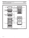

Philips Semiconductors Product data sheet
SC28L91
3.3 V or 5.0 V Universal Asynchronous
Receiver/Transmitter (UART)
2004 Oct 21
10
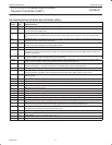
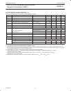
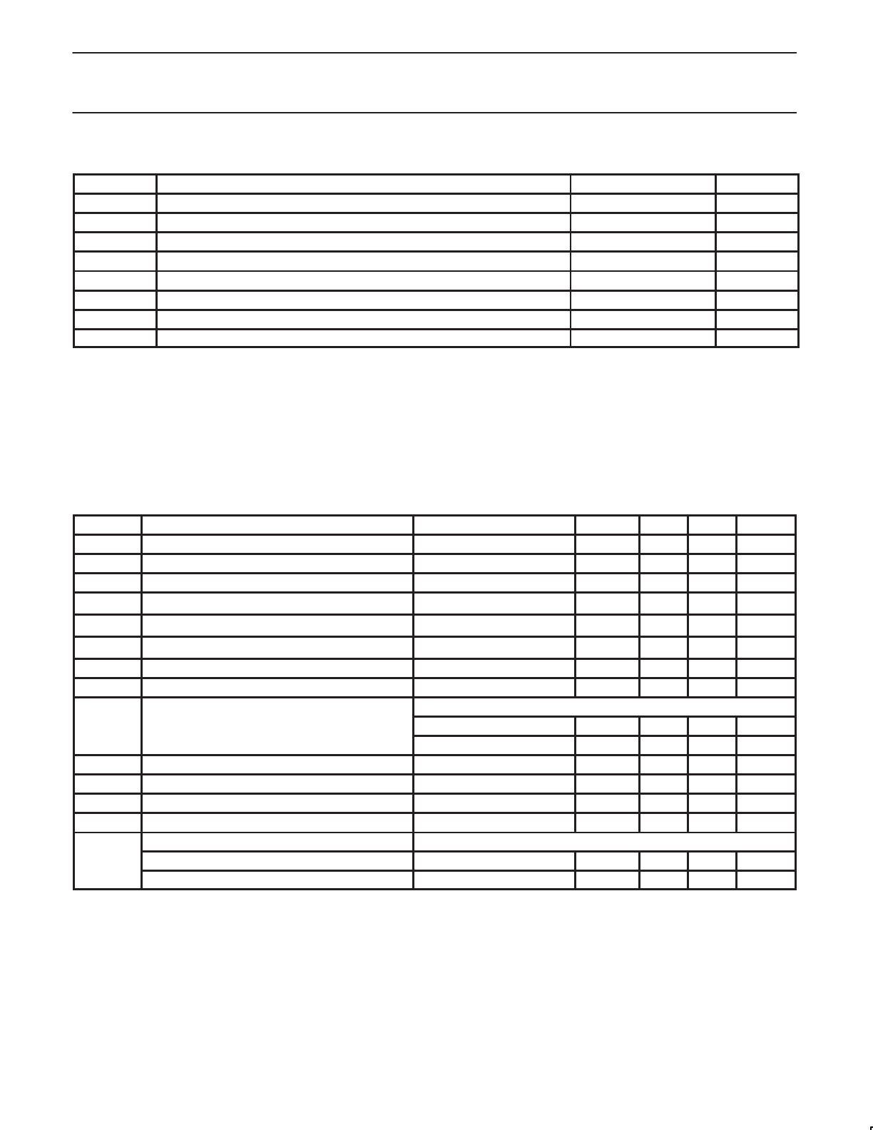
ABSOLUTE MAXIMUM RATINGS
1
Symbol
Parameter Rating Unit
T
amb
Operating ambient temperature range
2
Note 4 °C
T
stg
Storage temperature range –65 to +150 °C
V
CC
Voltage from V
CC
to GND
3
–0.5 to +7.0 V
V
S
Voltage from any pin to GND
3
–0.5 to V
CC
+0.5 V
P
D
Package power dissipation (PLCC44) 2.4 W
P
D
Package power dissipation (PQFP44) 1.78 W
Derating factor above 25 °C (PLCC44) 19 mW/°C
Derating factor above 25 °C (PQFP44) 14 mW/°C
NOTES:
1. Stresses above those listed under Absolute Maximum Ratings may cause permanent damage to the device. This is a stress rating only and
functional operation of the device at these or any other condition above those indicated in the operation section of this specification is not
implied.
2. For operating at elevated temperatures, the device must be derated based on +150°C maximum junction temperature.
3. This product includes circuitry specifically designed for the protection of its internal devices from damaging effects of excessive static
charge. Nonetheless, it is suggested that conventional precautions be taken to avoid applying any voltages larger than the rated maxima.
4. Parameters are valid over specified temperature and voltage range.
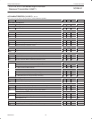
DC ELECTRICAL CHARACTERISTICS
1,
2,
3
V
CC
= 5 V ± 10 %, T
amb
= –40 °C to +85 °C, unless otherwise specified.
Symbol
Parameter Conditions Min Typ Max Unit
V
IL
Input low voltage 0.8 V
V
IH
Input high voltage (except X1/CLK) 2.4 1.5 V
V
IH
Input high voltage (X1/CLK) 0.8V
CC
2.4 V
V
OL
Output low voltage
I
OL
= 2.4 mA
0.2 0.4 V
V
OH
Output high voltage (except OD outputs)
4
I
OH
= –400 µA
V
CC
– 0.5 V
I
IX1PD
X1/CLK input current - power down
V
IN
= 0 V to V
CC
0.5 0.05 0.5 µA
I
ILX1
X1/CLK input low current - operating V
IN
= 0 V –130 0 µA
I
IHX1
X1/CLK input high current - operating V
IN
= V
CC
0 130 µA
Input leakage current:
I
I
All except input port pins V
IN
= 0 V to V
CC
–0.5 0.05 +0.5 µA
Input port pins
5
V
IN
= 0 V to V
CC
–8 0.05 +0.5 µA
I
OZH
Output off current high, 3-State data bus V
IN
= V
CC
0.5 µA
I
OZL
Output off current low, 3-State data bus V
IN
= 0 V –0.5 µA
I
ODL
Open-drain output low current in off-state V
IN
= 0 V –0.5 µA
I
ODH
Open-drain output high current in off-state V
IN
= V
CC
0.5 µA
Power supply current
6
I
CC
Operating mode CMOS input levels 7 25 mA
Power down mode CMOS input levels ≤1 5
mA
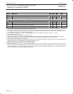
NOTES:
1. Parameters are valid over specified temperature and voltage range.
2. All voltage measurements are referenced to ground (GND). For testing, all inputs swing between 0.4 V and 3.0 V with a transition time of
5 ns maximum. For X1/CLK, this swing is between 0.4 V and 0.8V
CC
. All time measurements are referenced at input voltages of 0.8 V and
2.0 V and output voltages of 0.8 V and 2.0 V, as appropriate.
3. Typical values are at +25 °C, typical supply voltages, and typical processing parameters.
4. Test conditions for outputs: C
L
= 125 pF, except open drain outputs. Test conditions for open drain outputs: C
L
= 125 pF,
constant current source = 2.6 mA.
5. Input port pins have active pull-up transistors that will source a typical 2 µA from V
CC
when the input pins are at V
SS
.
Input port pins at V
CC
source 0.0 µA.
6. All outputs are disconnected. Inputs are switching between CMOS levels of V
CC
– 0.2 V and V
SS
+ 0.2 V.