


Philips Semiconductors Product data sheet
SC28L91
3.3 V or 5.0 V Universal Asynchronous
Receiver/Transmitter (UART)
2004 Oct 21
14
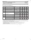
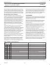
AC CHARACTERISTICS (3.3 VOLT)
1,
2,
3,
4
V
CC
= 3.3 V ± 10 %, T
amb
= –40 °C to +85 °C, unless otherwise specified.
Symbol Parameter Min Typ Max Unit
Reset Timing (See Figure 4)
t
RES
Reset pulse width 100 20 ns
Bus Timing
5
(See Figure 5)
t
*AS
A0–A3 setup time to RDN, WRN Low 10 6 ns
t
*AH
A0–A3 hold time from RDN, WRN low 33 ns
t
*CS
CEN setup time to RDN, WRN low 0 ns
t
*CH
CEN Hold time from RDN. WRN low 0 ns
t
*RW
WRN, RDN pulse width (Low time) 20 10 ns
t
*DD
Data valid after RDN low (125pF load. See Figure 3 for smaller loads.) 46 75 ns
t
*DA
RDN low to data bus active
6
0 ns
t
*DF
Data bus floating after RDN or CEN high 15 20 ns
t
*DI
RDN or CEN high to data bus invalid
7
0 ns
t
*DS
Data bus setup time before WRN or CEN high (write cycle) 43 ns
t
*DH
Data hold time after WRN high 0 –15 ns
t
*RWD
High time between read and/or write cycles
5,
7
27 ns
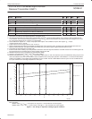
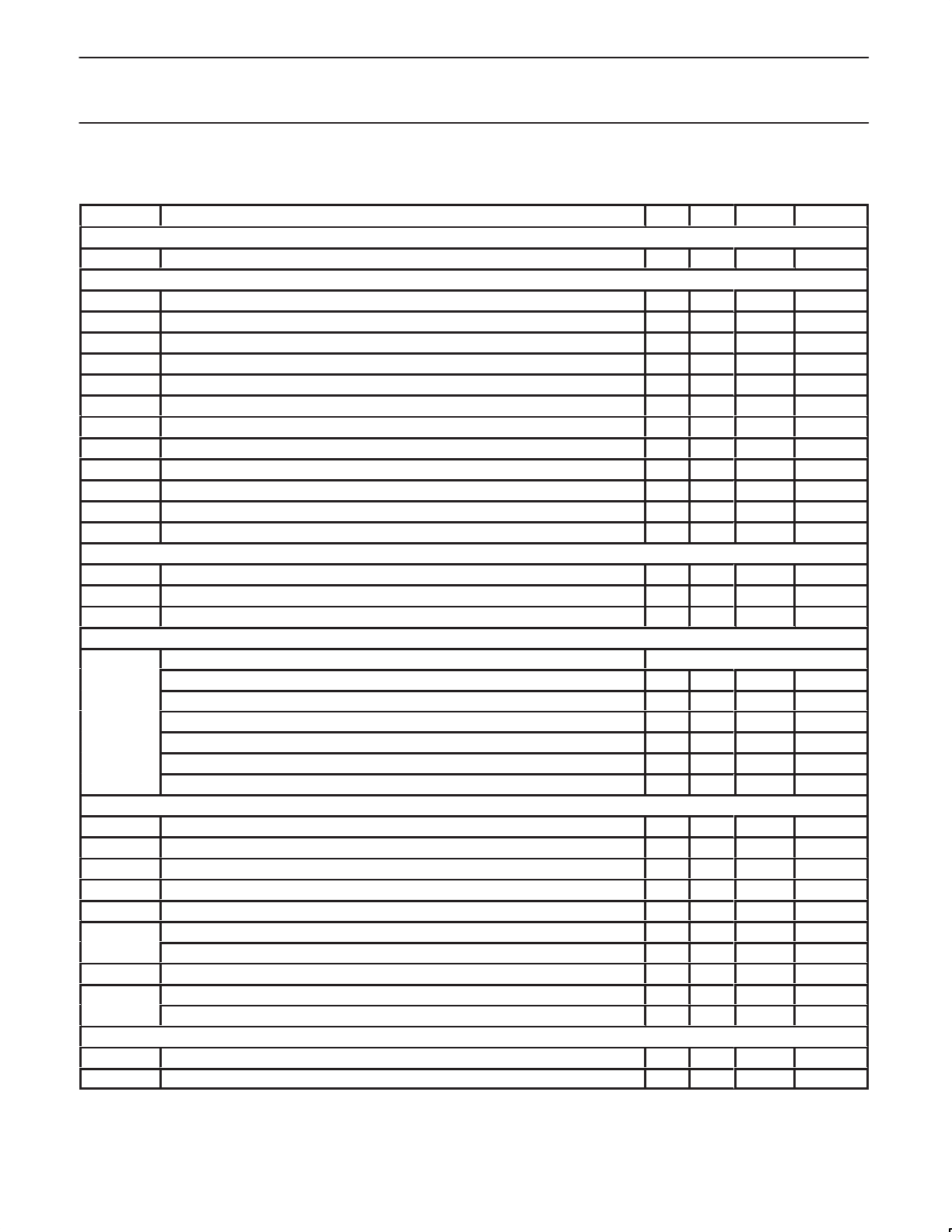
Port Timing
5
(See Figure 9)
t
*PS
Port in setup time before RDN low (Read IP ports cycle) 0 –20 ns
t
*PH
Port in hold time after RDN high 0 –20 ns
t
*PD
OP port valid after WRN or CEN high (OPR write cycle) 50 75 ns
Interrupt Timing (See Figure 10)
t
*IR
INTRN (or OP3–OP7 when used as interrupts) negated from:
Read RxFIFO (RxRDY/FFULL interrupt) 40 79 ns
Write TxFIFO (TxRDY interrupt) 40 79 ns
Reset Command (delta break change interrupt) 40 79 ns
Stop C/T command (Counter/timer interrupt) 40 79 ns
Read IPCR (delta input port change interrupt) 40 79 ns
Write IMR (Clear of change interrupt mask bit(s)) 40 79 ns
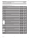
Clock Timing (See Figure 11)
t
*CLK
X1/CLK high or low time 35 25 ns
f
*CLK
X1/CLK frequency
8
(for higher speeds contact factory) 0.1 3.686 8 MHz
f
*CTC
C/T Clk (IP2) high or low time (C/T external clock input) 30 15 ns
f
*CTC
C/T Clk (IP2) frequency
8
(for higher speeds contact factory) 0 8 MHz
t
*RX
RxC high or low time (16X) 30 10 ns
f
*RX
RxC Frequency (16X) (for higher speeds contact factory) 0 16 MHz
RxC Frequency (1x)
8,
9
0 1 MHz
t
*TX
TxC High or low time (16X) 30 15 ns
f
*TX
TxC frequency (16X) (for higher speeds contact factory) 16 MHz
TxC frequency (1X)
8,
9
0 1 MHz
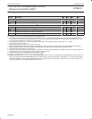
Transmitter Timing, external clock (See Figure 12)
t
*TXD
TxD output delay from TxC low (TxC input pin) 40 78 ns
t
*TCS
Output delay from TxC output pin low to TxD data output 8 30 ns