


Philips Semiconductors Product data sheet
SC28L91
3.3 V or 5.0 V Universal Asynchronous
Receiver/Transmitter (UART)
2004 Oct 21
11
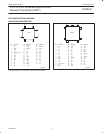
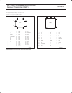
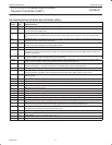
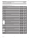
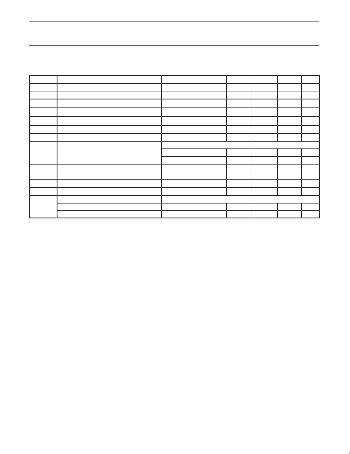
DC ELECTRICAL CHARACTERISTICS
1,
2,
3
V
CC
= 3.3 V ± 10 %, T
amb
= –40 °C to +85 °C, unless otherwise specified.
Symbol
Parameter Conditions Min Typ Max Unit
V
IL
Input low voltage 0.65 0.2*V
CC
V
V
IH
Input high voltage 0.8*V
CC
1.7 V
V
OL
Output low voltage
I
OL
= 2.4 mA
0.2 0.4 V
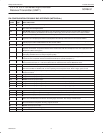
V
OH
Output high voltage (except OD outputs)
4
I
OH
= –400 µA
V
CC
– 0.5 V
CC
– 0.2 V
I
IX1PD
X1/CLK input current - power down
V
IN
= 0 V to V
CC
–0.5 0.05 +0.5 µA
I
ILX1
X1/CLK input low current - operating V
IN
= 0 V –80 0 µA
I
IHX1
X1/CLK input high current - operating V
IN
= V
CC
0 80 µA
Input leakage current:
I
I
All except input port pins V
IN
= 0 V to V
CC
–0.5 0.05 +0.5 µA
Input port pins
5
V
IN
= 0 V to V
CC
–8 0.5 +0.5 µA
I
OZH
Output off current high, 3-State data bus V
IN
= V
CC
0.5 µA
I
OZL
Output off current low, 3-State data bus V
IN
= 0 V –0.5 µA
I
ODL
Open-drain output low current in off-state V
IN
= 0 V –0.5 µA
I
ODH
Open-drain output high current in off-state V
IN
= V
CC
0.5 µA
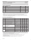
Power supply current
6
I
CC
Operating mode CMOS input levels 5 mA
Power down mode CMOS input levels ≤1 5.0
mA
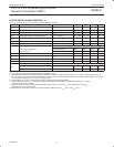
NOTES:
1. Parameters are valid over specified temperature and voltage range.
2. All voltage measurements are referenced to ground (GND). For testing, all inputs swing between 0.4 V and 3.0 V with a transition time of
5 ns maximum. For X1/CLK, this swing is between 0.4 V and 0.8*V
CC
. All time measurements are referenced at input voltages of 0.8 V and
2.0 V and output voltages of 0.8 V and 2.0 V, as appropriate.
3. Typical values are at +25 °C, typical supply voltages, and typical processing parameters.
4. Test conditions for outputs: C
L
= 125 pF, except open drain outputs. Test conditions for open drain outputs: C
L
= 125 pF,
constant current source = 2.6 mA.
5. Input port pins have active pull-up transistors that will source a typical 2 µA from V
CC
when the input pins are at V
SS
.
Input port pins at V
CC
source 0.0 µA.
6. All outputs are disconnected. Inputs are switching between CMOS levels of V
CC
– 0.2 V and V
SS
+ 0.2 V.