


Philips Semiconductors Product data sheet
SC28L91
3.3 V or 5.0 V Universal Asynchronous
Receiver/Transmitter (UART)
2004 Oct 21
20
latency is longer than the pause in the data stream.) In this case,
when a new character has been received, the counter/timer will be
restarted by the receiver, thereby withdrawing its interrupt. If, at this
time, the interrupt service begins for the previously seen interrupt, a
read of the ISR will show the “Counter Ready” bit not set. If nothing
else is interrupting, this read of the ISR will return a x’00 character.
Multi-drop Mode (9-bit or Wake-Up)
The UART is equipped with a wake up mode for multi-drop
applications. This mode is selected by programming bits MR1[4:3]or
to ‘11’. In this mode of operation, a ‘master’ station transmits an
address character followed by data characters for the addressed
‘slave’ station. The slave station(s) whose receiver(s) that are
normally disabled, examine the received data stream and ‘wakeup’
the CPU (by setting RxRDY) only upon receipt of an address
character. The CPU compares the received address to its station
address and enables the receiver if it wishes to receive the
subsequent data characters. Upon receipt of another address
character, the CPU may disable the receiver to initiate the process
again.
A transmitted character consists of a start bit, the programmed
number of data bits, and Address/Data (A/D) bit, and the
programmed number of stop bits. The polarity of the transmitted A/D
bit is selected by the CPU by programming bit MR1[2]. MR1[2]= 0
transmits a zero in the A/D bit position, which identifies the
corresponding data bits as data. MR1[2] = 1 transmits a one in the
A/D bit position, which identifies the corresponding data bits as an
address. The CPU should program the mode register prior to
loading the corresponding data bits into the TxFIFO.
MR1[2] = 1 transmits a one in the A/D bit position, which identifies
the corresponding data bits as an address. The CPU should
program the mode register prior to loading the corresponding data
bits into the TxFIFO.
In this mode, the receiver continuously looks at the received data
stream, whether it is enabled or disabled. If disabled, it sets the
RxRDY status bit and loads the character into the RxFIFO if the
received A/D bit is a one (address tag), but discards the received
character if the received A/D bit is a zero (data tag). If enabled, all
received characters are transferred to the CPU via the RxFIFO. In
either case, the data bits are loaded into the data FIFO while the
A/D bit is loaded into the status FIFO position normally used for
parity error (SR[5] ). Framing error, overrun error, and break detect
operate normally whether or not the receiver is enabled.
PROGRAMMING
The operation of the UART is programmed by writing control words
into the appropriate registers. Operational feedback is provided via
status registers which can be read by the CPU. The addressing of
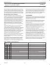
the registers is described in Table 1.
The contents of certain control registers are initialized to zero on
RESET. Care should be exercised if the contents of a register are
changed during operation, since certain changes may cause
operational problems.
For example, changing the number of bits per character while the
transmitter is active may cause the transmission of an incorrect
character. In general, the contents of the MR, the CSR, and the
OPCR should only be changed while the receiver(s) and
transmitter(s) are not enabled, and certain changes to the ACR
should only be made while the C/T is stopped.
The channel has 3 mode registers (MR0, 1, 2) which control the
basic configuration of the channel. Access to these registers is
controlled by independent MR address pointers. These pointers are
set to 0 or 1 by MR control commands in the command register
“Miscellaneous Commands”. Each time the MR registers are
accessed the MR pointer increments, stopping at MR2. It remains
pointing to MR2 until set to 0 or 1 via the miscellaneous commands
of the command register. The pointer is set to 1 on reset for
compatibility with previous Philips Semiconductors UART software.
Refer to Table 2 for register bit descriptions. The reserved registers
at addresses 0x02 and 0x0A should never be read during normal
operation since they are reserved for internal diagnostics.
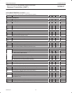
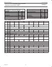
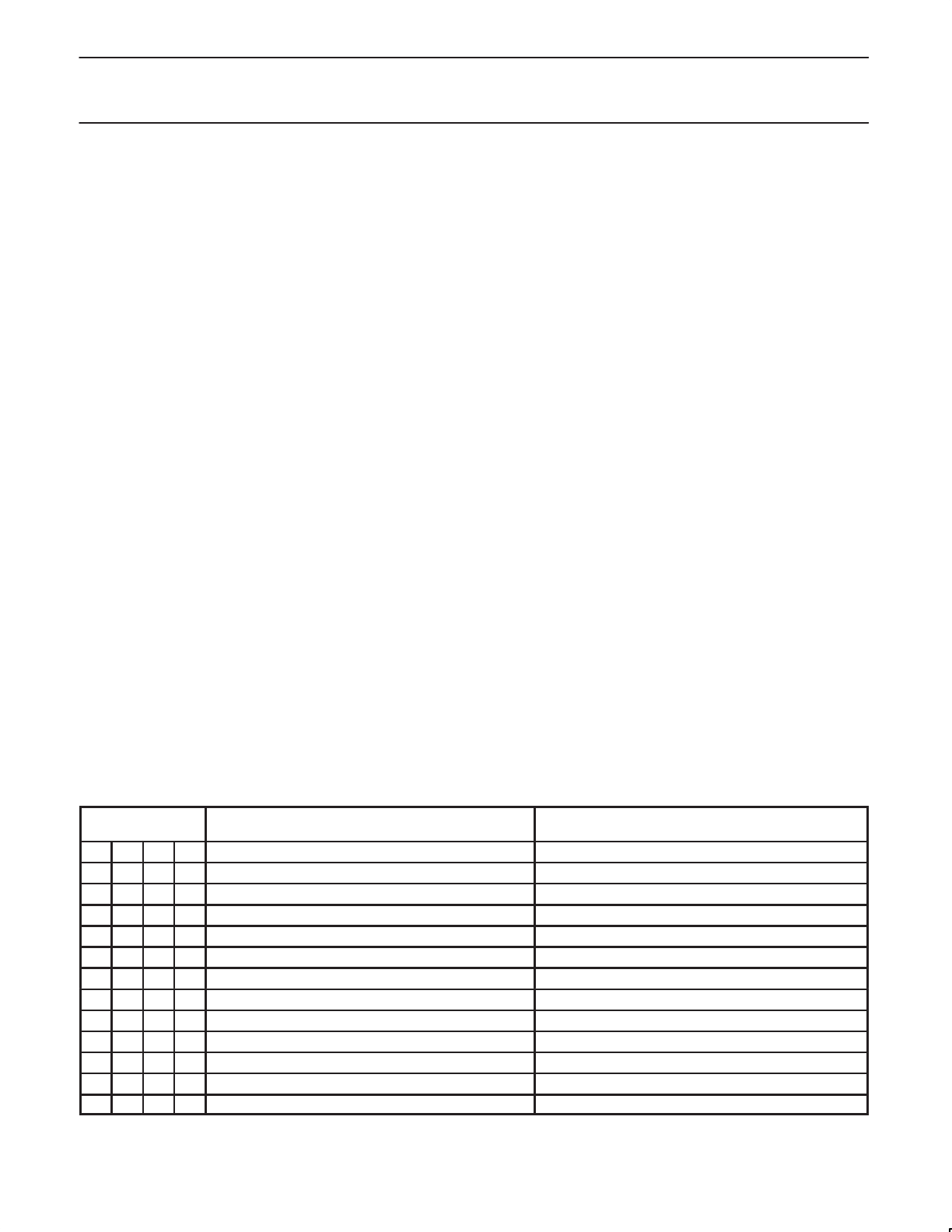
Table 1. SC28L91 register addressing
Address Bits
A[3:0]
READ (RDN = 0) WRITE (WRN = 0)
0 0 0 0 Mode Register(MR0, MR1, MR2) Mode Register(MR0, MR1, MR2)
0 0 0 1 Status Register(SR) Clock Select Register(CSR)
0 0 1 0 Reserved Command Register(CR)
0 0 1 1 Rx Holding Register(RxFIFO) Tx Holding Register(RxFIFO)
0 1 0 0 Input Port Change Register (IPCR) Aux. Control Register (ACR)
0 1 0 1 Interrupt Status Register (ISR) Interrupt Mask Register (IMR)
0 1 1 0 Counter/Timer Upper (CTU) C/T Upper Preset Register (CTPU)
0 1 1 1 Counter/Timer Lower (CTL) C/T Lower Preset Register (CTPL)
1 1 0 0 Interrupt vector (68K mode), Misc. register in Intel mode Interrupt vector (68K mode), Misc. register in Intel mode
1 1 0 0 IVR Motorola mode, Misc. register (Intel mode) IVR Motorola mode, Misc. register (Intel mode)
1 1 0 1 Input Port (IPR) Output Port Configuration Register (OPCR)
1 1 1 0 Start Counter Command Set Output Port Bits Command (SOPR)
1 1 1 1 Stop Counter Command Reset output Port Bits Command (ROPR)
NOTE:
1. The three MR registers are accessed via the MR Pointer and Commands 0x1n and 0xBn (where n = represents receiver and transmitter enable bits)