


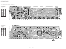
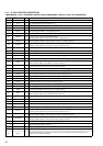
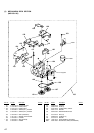
38
Pin No. Pin Name I/O Description
73 X1A O
Sub system clock output terminal (32.768 kHz)
74 X0A I
Sub system clock input terminal (32.768 kHz)
75 DAVN I
Data transmit completed detection signal input from the RDS decoder (IC50) “H” active
76 CDON-ON I
CD/MD on/off control signal input terminal (fixed at “L” in this set)
77 BU-IN
I
Battery detection signal input from the SONY bus interface (IC500) and battery detect circuit
“L” is input at low voltage
78 DSPREADY
I
Transfer enable signal input from the CXD2726Q (IC100)
“L”: transfer prohibition , “H”: transfer permission
79 KEYACK
I
Input of acknowledge signal for the key entry Acknowledge signal is input to accept function
and eject keys in the power off status On at input of “H”
80 AD ON
O
A/D converter power control signal output terminal
When the KEYACK (pin
ul
) that controls reference voltage power for key A/D conversion input
is active, “L” is output from this terminal to enable the input
81 ACCIN
I Accessory detection signal input terminal “L”: accessory on
82
FLASH ON O
Power on/off control signal output of the illumination LED and liquid crystal display driver
(IC800) “H”: power on
83 PW-ON
O Main system power supply on/off control signal output terminal “H”: power on
84 TESTIN
I Setting terminal for the test mode “L”: test mode, Normally: fixed at “H”
85 RAMBU I
Internal RAM reset detection signal input from the RAM reset (IC570)
Input terminal to check that RAM data are not destroyed due to low voltage
This checking is made within 100 msec after reset
86 HSTX I
Hardware standby input terminal “L”: hardware standby mode Reset signal input in this set
87 MD2 I
Setting terminal for the CPU operational mode (fixed at “L” in this set)
88 MD1 I
Setting terminal for the CPU operational mode (fixed at “H” in this set)
89 MD0 I
Setting terminal for the CPU operational mode (fixed at “H” in this set)
90 RESET I
System reset signal input from the reset signal generator (IC560) and reset switch (S500)
“L”: reset “L” is input for several 100 msec after power on, then it changes to “H”
91 VSS —
Ground terminal
92 X0
I Main system clock input terminal (3.68 MHz)
93 X1
O Main system clock output terminal (3.68 MHz)
94 VCC —
Power supply terminal (+5V)
95 ILLIN
I
Auto dimmer control illumination line detection signal input terminal
“L” is input at dimmer detection
96
TELATT I Telephone detection signal input terminal At input of “H”, the signal is attenuated by –20 dB
97
EMPH I Emphasis control signal input terminal Not used (open)
98
F CH O Frequency changing terminal “H”: frequency change Not used (open)
99 to 102 NC O
Not used (open)
103 4V SEL I
Input terminal of whether line driver is mounted or not is detected
“L”: line driver is not mounted, “H”: line driver is mounted
104 COL SEL
I
Setting terminal for the illumination color
“L”: 2 color (XR-C7500R), “H”: 1 color (XR-C7500RX)
105 AMPATT
O Power amplifier muting on/off control signal output terminal “H”: muting on
106 BOOT
O Serial data output to the liquid crystal display drive controller (IC800)
107 DSP GAIN
O Not used (open)
108 NC
O Not used (open)
109 XR CDMD
I
Setting terminal for the internal mechanism tape or CD/MD
“L”: tape, “H”: CD/MD (fixed at “L” in this set)
110 DSP ON
O Power supply on/off control signal output terminal “H”: DSP on Not used (open)