


2
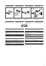
TABLE OF CONTENTS
1. SERVICING NOTES ............................................... 2
2. GENERAL
Location of Controls ....................................................... 3
Setting the Clock ............................................................. 3
Installation ....................................................................... 4
Connections ..................................................................... 6
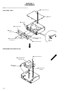
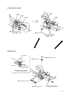
3. DISASSEMBLY ......................................................... 10
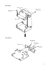
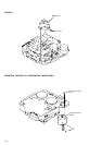
4. ASSEMBLY OF MECHANISM DECK........... 12
5. MECHANICAL ADJUSTMENTS ....................... 15
6. ELECTRICAL ADJUSTMENTS
Test Mode ........................................................................ 15
Tape Deck Section .......................................................... 16
Tuner Section .................................................................. 16
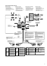
7. DIAGRAMS
7-1. Block Diagram – TUNER/TAPE Section – ................... 17
7-2. Block Diagram – MAIN Section – ................................. 18
7-3. Block Diagram
– DISPLAY/KEY CONTROL Section –........................ 19
7-4. Block Diagram
– BUS CONTROL/POWER SUPPLY Section – ........... 20
7-5. Note for Printed Wiring Boards and
Schematic Diagrams ....................................................... 21
7-6. Printed Wiring Board
– Main Board (Component Side) – ................................ 22
7-7. Printed Wiring Board
– Main Board (Conductor Side) – .................................. 23
7-8. Schematic Diagram – Main Board (1/4) – ..................... 24
7-9. Schematic Diagram – Main Board (2/4) – ..................... 25
7-10. Schematic Diagram – Main Board (3/4) – ..................... 26
7-11. Schematic Diagram – Main Board (4/4) – ..................... 27
7-12. Printed Wiring Board – SUB Board – ........................... 28
7-13. Schematic Diagram – SUB Board – ............................... 28
7-14. Printed Wiring Board – KEY Board –........................... 30
7-15. Schematic Diagram – KEY Board – .............................. 31
7-16. IC Pin Function Description ........................................... 34
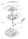
8. EXPLODED VIEWS ................................................ 40
9. ELECTRICAL PARTS LIST ............................... 43
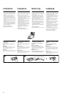
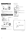
Notes on chip component replacement
• Never reuse a disconnected chip component.
• Notice that the minus side of a tantalum capacitor may be dam-
aged by heat.
Flexible Circuit Board Repairing
• Keep the temperature of the soldering iron around 270 ˚C dur-
ing repairing.
• Do not touch the soldering iron on the same conductor of the
circuit board (within 3 times).
• Be careful not to apply force on the conductor when soldering
or unsoldering.
SECTION 1
SERVICING NOTES
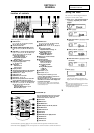
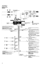
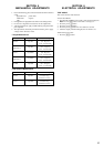
MODEL IDENTIFICATION
The XR-C7500R and XR-C7500RX have three types of MAIN
boards respectively.
TUX1
R606
R607
CN201
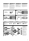
– MAIN BOARD (Conductor Side) –
TYPE A TYPE B TYPE C
R606 × aa
R607 a × a