


2929
MZ-B100
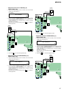
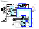
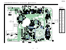
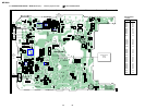
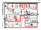
• Main board is four-layer printed board.
However, the patterns of layers 2 and 3 have not been
included in this diagrams.
• Replacement of IC801 used in this set requires a special
tool.
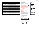
• Lead Layouts
surface
Lead layout of conventional IC CSP (chip size package)
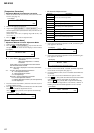
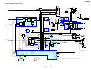
Note on Printed Wiring Board:
• X : parts extracted from the component side.
• Y : parts extracted from the conductor side.
• x : parts mounted on the conductor side.
•
z
: Through hole.
• : Pattern from the side which enables seeing.
(The other layers' patterns are not indicated.)
Caution:
Pattern face side: Parts on the pattern face side seen from
(Conductor Side) the pattern face are indicated.
Parts face side: Parts on the parts face side seen from
(Component Side) the parts face are indicated.
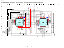
Note on Schematic Diagram:
• All capacitors are in µF unless otherwise noted. pF: µµF
50 WV or less are not indicated except for electrolytics
and tantalums.
• All resistors are in Ω and
1
/
4
W or less unless otherwise
specified.
• % : indicates tolerance.
•
f
: internal component.
• A : B+ Line.
• Power voltage is dc 3 V and fed with regulated dc power
supply from external power voltage jack.
• Voltages and waveforms are dc with respect to ground
under no-signal conditions.
no mark : PLAYBACK
( ) : RECORD
∗
: Impossible to measure
• Voltages are taken with a VOM (Input impedance 10 MΩ).
Voltage variations may be noted due to normal produc-
tion tolerances.
• Waveforms are taken with a oscilloscope.
Voltage variations may be noted due to normal produc-
tion tolerances.
• Circled numbers refer to waveforms.
• Signal path.
E : PLAYBACK
j : PLAYBACK (ANALOG IN)
l : RECORD (DEGITAL IN)
• Replacement of IC801 used in this set requires a special
tool.
• The voltage and waveform of CSP (chip size package)
cannot be measured, because its lead layout is different
form that of conventional IC.
Note: The components identified by mark 0 or dotted line
with mark 0 are critical for safety.
Replace only with part number specified.
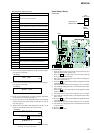
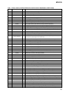
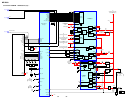
Pin No. Pin name I/O Description
220 XRST MTR DRV O Reset control signal output to the motor driver (IC701)
221 XRF RST O Reset control signal output to RF amp (IC501)
222 MCUVDD3 — Power supply terminal (for the microcomputer block) (+1.5V)
223 SPDL MON I Spindle servo monitor signal input from the motor driver (IC701)
224 XAVLS I Input terminal for AVLS switch detection signal
225, 226 JOG A, B I Jog dial pulse input terminal from the switch & LCD module
227 XHOLD SW I HOLD switch (S801) input terminal “L”: hold ON, “H”: hold OFF
228 SYNC REC I SYNCHRO REC switch (S802) input terminal “L”: OFF, “H”: ON Not used (open)
229 TSB SSB CTL O TSB/SSB changeover control signal output Not used (open)
230 PROTECT I
Detection input terminal of the record check claw from the protect detection switch (S803)
“L”: recording possible condition, “H”: protect
231 FLASHVDD — Power supply terminal (for the internal FLASH ROM) (+2.4V)
232 FLASHVSS — Ground terminal (for the internal FLASH ROM)
233 SLD MON I Sled servo monitor signal input from the motor driver (IC701)
234 VLON O Power supply control signal output for the laser diode drive to the power control (IC901)
235 SLEEP O System sleep control signal output to the power control (IC901) “H”: sleep ON
236 FFCLR O Input latch output for the start switching to the power control (IC901)
237 CHG GAIN O Charge gain control signal output to the power control (IC601)
238 CHG O Charge ON/OFF control signal output to the power control (IC601) “H”: charge ON
239 TUN REG ON O Not used (open)
240 XHP STBY O Power supply control signal output terminal for the headphone amp Not used (open)
241 MIFVDD3 — Power supply terminal (for the microcomputer I/F block) (+2.3V)
242 MIFVSS2 — Ground terminal (for the microcomputer I/F block)
243 TEST2 I Input terminal for the main test (normally open)
244 NC — Not used (open)
z
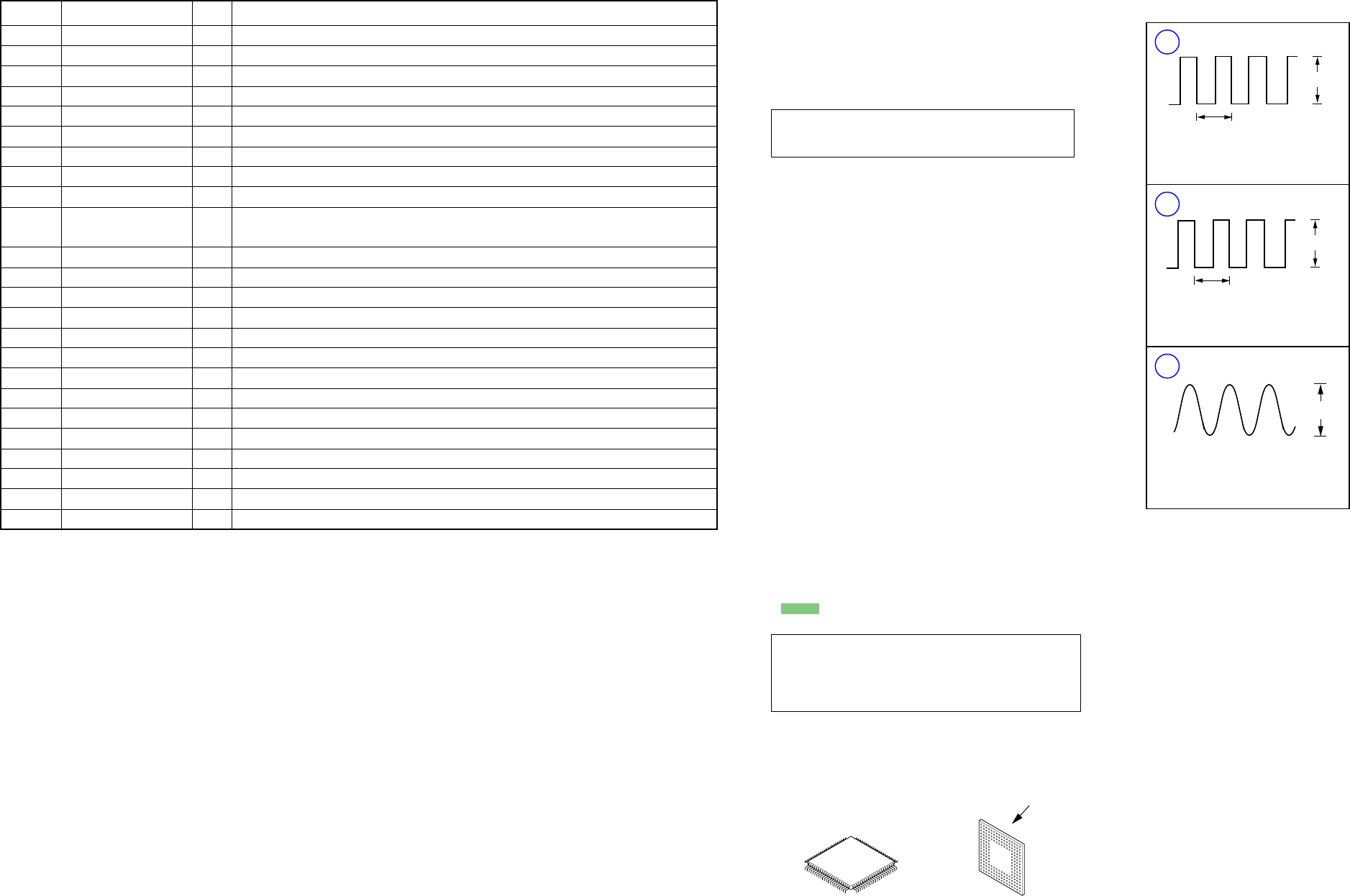
Waveforms
1
2
3
IC601 4
XIN
VOLT/DIV : 0.5 V AC
TIME/DIV : 0.1 µsec
IC901 th
CLK
IC801 wg
OSCO
VOLT/DIV : 0.5 V AC
TIME/DIV : 0.1 µsec
VOLT/DIV :0.5 V AC
TIME/DIV : 20 nsec
2.3Vp-
p
0.56 sec
2.3Vp-
p
0.56 sec
2.2Vp-
p
45.1584MHz