


27
MZ-B100
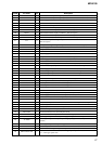
Pin No. Pin name I/O Description
101 SLCV I Sled motor drive comparison signal input (V) from the motor driver (IC701)
102 SLCW I Sled motor drive comparison signal input (W) from the motor driver (IC701)
103 DIFVDD1 — Power supply terminal (for DSP I/F) (+2.3V)
104 DIFVSS1 — Ground terminal (for DSP I/F)
105 EFMO O EFM encode data output for the record to the over write head drive (IC601)
106 MNT0 O Internal DSP monitor output (0) terminal Not used (open)
107 MNT1 O Internal DSP monitor output (1) terminal Not used (open)
108 MNT2 O Internal DSP monitor output (2) terminal Not used (open)
109 MNT3 O Internal DSP monitor output (3) terminal Not used (open)
110 SENSE O Internal DSP (SENS) monitor output terminal Not used (open)
111 TX O
Record data output enable signal output monitor terminal of the internal DSP
Not used (open)
112 RECP O Laser power changeover signal output monitor terminal Not used (open)
113 DSPVDD3 — Power supply terminal (for DSP block) (+1.5V)
114 to 117 NC O Output terminal for the external D-RAM Not used (open)
118 DRAMVSS0 — Ground terminal (for the external D-RAM)
119 DRAMVDD0 — Power supply terminal (for the external D-RAM) (+2.4V)
120 to 138 NC O Output terminal for the external D-RAM Not used (open)
139 DRAMVDD1 — Power supply terminal (for the external D-RAM) (+2.4V)
140 DRAMVSS1 — Ground terminal (for the external D-RAM)
141 TSB MST VDD — Power supply terminal (for TSB master communication) (+2.8V)
142 RMC DTCK I/O TSB serial data input/output with the remote commander attached headphone
143 TSB SLV VDD — Power supply terminal (for I/F to TSB slave communication)
144 TSB SLVI I TSB slave signal input from the remote commander attached headphone
145 TSB SLVO O TSB slave signal output to the remote commander attached headphone
146 TDI I Data input terminal for JTAG Not used (open)
147 TMS I Test mode control input terminal for JTAG Not used (open)
148 TCK I Clock input terminal for JTAG Not used (open)
149 XTRST I Reset input terminal for JTAG Not used (open)
150 TDO O Data output terminal for JTAG Not used (open)
151 JTAGVDD — Power supply terminal (for JTAG) (+2.4V)
152 JTAGVSS — Ground terminal (for JTAG)
153 MCUVDD2 — Power supply terminal (for the microcomputer block) (+1.5V)
154 MIFVDD0 — Power supply terminal (for the microcomputer I/F block) (+2.3V)
155 MIFVSS0 — Ground terminal (for the microcomputer I/F block)
156, 157 TEST1, TEST0 I Input terminal for the main test (normally fixed at “L”)
158 EVA I EVA/FLASH chip discrimination terminal “L”: FLASH chip, “H”: EVA chip
159 OPR LED — Not used (open)
160 SSB DATA I/O Input/output of SSB data with RF amp (IC501)
161 SSB CLK O SSB clock output to RF amp (IC501)
162 MCUVSS0 — Ground terminal (for the microcomputer block)
163 VREC PWM O Over write head control spare terminal Not used (open)
164 VL PWM O PWM signal output for the laser power supply voltage control to the power control (IC901)
165 VC PWM O
PWM signal output for the system power supply voltage control to the power control
(IC901)
166 SPDL AUX PWM O PWM signal output for the spindle support to the motor driver (IC701)
167, 168 NC O Not used (open)
169 CLK SEL O System clock select signal output to the power control (IC901)
170 OPEN CLOSE SW I
Open/close detection switch (S806) of the upper panel input terminal
“L”: when upper panel close