


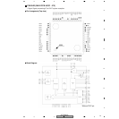
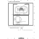
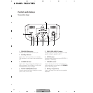
SE-DIR800C
52
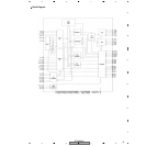
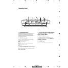
1234
1234
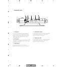
C
D
F
A
B
E
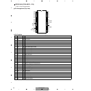
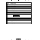
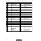
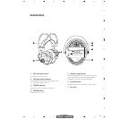
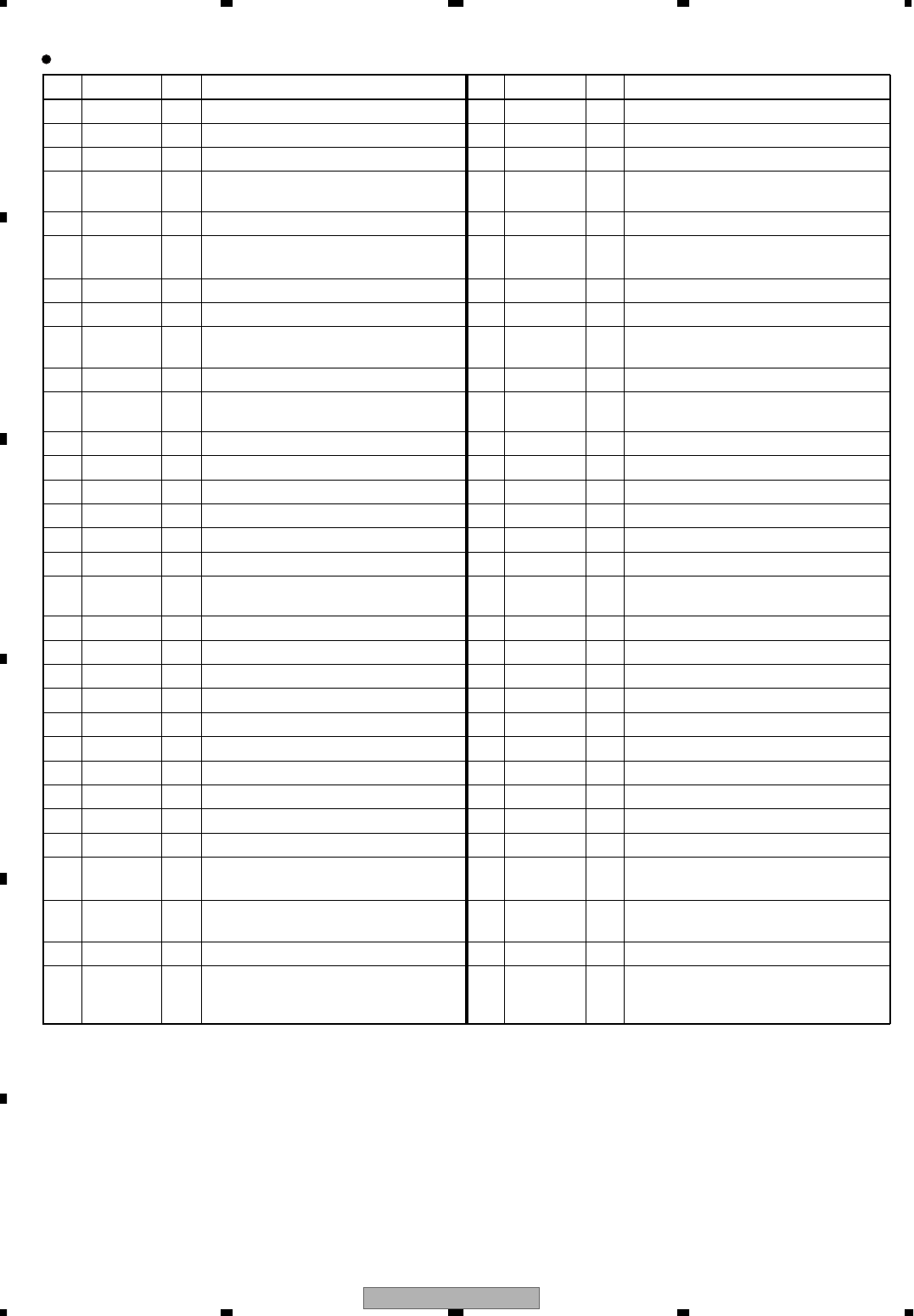
Pin Function
No. Pin Name I/O Function No. Pin Name I/O Function
1 TEST12 I Test pin, normally fixed to L 33 CSOD O Chapter start delayed output
2 TEST13 I Test pin, normally fixed to H 34 SRDT O Read-out output of serial interface data
3 TEST14 I Test pin, normally fixed to H 35 SWDT I Writing input of serial interface data
4 VDDE
−
Digital I/O power supply 36 XSCEN I
Enable input of serial interface data
(negative logic)
5 VSS
−
Digital GND 37 SCLK I Clock input of serial interface data
6 ADVRH I
Reference voltage input for RF A/D
converter (high)
38 SCMODE I
Control mode selection (L: Pin setting, H:
Serial setting)
7 ADAVS
−
Analog GND for RF A/D converter 39 VSS
−
Digital GND
8 ADAVD
−
Analog power supply for RF A/D converter 40 OSCI I Crystal resonator circuit input (12.288MHz)
9 ADVRL I
Reference voltage input for RF A/D
converter (low)
41 VDDE
−
Digital I/O power supply
10 ADVIN I RF A/D converter input 42 VSS
−
Digital GND
11 VDDE
−
Digital I/O power supply 43 OSCO O
Crystal resonator circuit output
(12.288MHz)
12 VSS
−
Digital GND 44 TEST0 I Test pin, normally fixed to L
13 XRST I Reset (negative logic) 45 TEST1 I Test pin, normally fixed to L
14 DIFM0 I Select the audio output type 46 TEST2 I Test pin, normally fixed to L
15 DIFM1 I Select the audio output type 47 TEST3 I Test pin, normally fixed to L
16 TEST15 I Test pin, normally fixed to L 48 TEST4 I Test pin, normally fixed to L
17 PLREF O PLL reference output (fs) 49 TEST5 I Test pin, normally fixed to L
18 PLVAR O
PLL dividing output (256 dividing of APX
output or VCOR input)
50 TEST6 I Test pin, normally fixed to L
19 TEST16 I Test pin, normally fixed to L 51 TEST7 I Test pin, normally fixed to L
20 APVCI I PLL VCO control voltage input 52 TEST8 O Test pin, normally open-circuit
21 VSS
−
Digital GND 53 TEST9 O Test pin, normally open-circuit
22 APCPO O PLL charge pump 54 BCK O Bit clock output
23 APAVD
−
Power supply for PLL VCO 55 TEST10 O Test pin, normally open-circuit
24 APAVS
−
GND for PLL VCO 56 VDDE
−
Digital I/O power supply
25 VSS
−
Digital GND 57 VSS
−
Digital GND
26 VDDI
−
Digital internal power supply 58 VDDI
−
Digital internal power supply
27 VDDE
−
Digital I/O power supply 59 LRCK O Audio sampling clock output
28 VCOR I Clock input for data output 60 DAOUT O Data output for audio D/A converter
29 CHNUM I Channel number selection (L: 0ch,H: 1ch) 61 DTVALID O
Data valid flag output
(DTVALID, L: valid, H: Invalidity)
30 DIVCODE I
Full/Half band mode selection
(L: Full-band, H: Half-band)
62 EMPFS0 O Emphasis, fs information output
31 APX 0 PLL VCO output 63 EMPFS1 O Emphasis, fs information output
32 EXTCK I
Clock selection for data output
(L: APX internal connection, H: VCOR pin
input)
64 TEST11 I Test pin, normally fixed to H