© National Instruments Corporation B-1 NI PXI-4224 User Manual
B
Timing Signal Information
This appendix contains additional information about the timing signals
discussed in Chapter 4, Theory of Operation.
Connecting Timing Signals
Caution Exceeding the maximum input voltage ratings listed in Appendix A,
Specifications, can damage the device and the computer. NI is not liable for any damage
resulting from such signal connections.
Programmable Function Input Connections
You can externally control seven internal timing signals from PFI 0 and the
PXI trigger bus pins. The source for each of these signals is software
configurable from PFI 0, PXI_Trig<0..5>, or PXI_Star when you want
external control. This flexible routing scheme reduces the need to change
the physical wiring to the device I/O connector for applications requiring
alternative wiring.
As an input, each PFI signal can be individually configured for edge or level
detection and polarity selection. You can use the polarity selection for any
timing signal, but the edge or level detection depends on the particular
timing signal being controlled. The detection requirements for each timing
signal are listed in the corresponding sections.
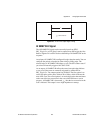
In edge-detection mode, the minimum pulse width required is 10 ns. This
requirement applies for both rising-edge and falling-edge polarity settings.
There is no maximum pulse width requirement in edge-detection mode.
In level-detection mode, there are no pulse width requirements imposed by
the PFIs themselves. Limits can be imposed by the particular timing signal
being controlled. These requirements are listed in the sections that describe
the signals.


