


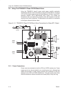
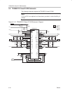
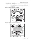
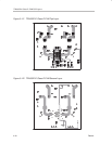
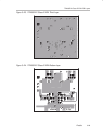


TPA005D12 Class-D EVM Interconnects
3-24
Details
3.7 TPA005D12 Class-D EVM Interconnects
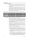
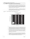
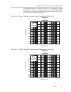
Table 3–4 shows the correlation between the TPA005D12 class-D amplifier IC
pins, the EVM pins, and the plug-n-play (PNP) platform sockets.
Table 3–4.TPA005D12 Class-D EVM/Plug-N-Play Platform Interconnects
CLASS-D EVM PLUG-N-PLAY PLATFORM
IC PIN EVM PIN FUNCTION ON EVM PNP SOCKET FUNCTION ON PLATFORM
8, 9 16, 21, 28 VDD Power for left channel, input, and
headphone circuits
VDD Power from J1, J2, J6, or B1
40, 33 VDD2 Power for right channel circuits VDD Power from J1, J2, J6, or B1
3, 7, 12, 13, 20,
27, 36, 37, 46,
47
GND Analog and power ground for EVM,
all pins
GND Ground for platform from J1, J2,
J6, or B1
44 RIN+ Class-D right channel positive input Right In (line) Right channel input from J3 or J4
45 RIN– Class-D right channel inverted input GND Ground for platform from J1, J2,
J6, or B1
38, 39 Rout+ Class-D right channel positive out-
put
Right Out + Right channel positive output to J7
or J8
34,35 Rout– Class-D right channel inverted out-
put
Right Out – Right channel negative output to
J7 or J8
5 LIN+ Class-D left channel positive input Left In (line) Left channel input from J4 or J5
4 LIN– Class-D left channel inverted input GND Ground for platform from J1, J2,
J6, or B1
10, 11 Lout+ Class-D left channel positive output Left Out + Left channel positive output to J8
or J9
14, 15 Lout– Class-D left channel inverted output Left Out – Left channel negative output to J8
or J9
2 Mute Mute control external input pin: ac-
tive low — selected amplifier active
when held > 2 V
N/C No connect
1 SD Shutdown control external input pin:
active low — normal operation when
held > 2 V
Mute Mute control from JP6 for use
when testing a headphone amplifi-
er in socket U5 in conjunction with
an EVM in U2/U3/U4
41 TP4 Fault–1: Logic level fault–1 output
signal. MSB. Open drain.
N/C No connect
42 TP3 Fault–0: Logic level fault–0 output
signal. LSB. Open drain.
N/C No connect