


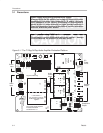
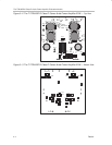
The TPA005D12 Class-D Audio Power Amplifier Evaluation Module
3-8
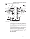
Details
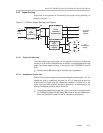
3.2.4 Class-D Differential Inputs
The TPA005D12 EVM line inputs allow the use of a single-ended or differential
audio source. The differential input stage of the amplifier cancels any noise
that appears on both input lines of a channel. To use the EVM with a differential
source, connect the positive lead of the audio source to the RIN+/LIN+ inputs
and the negative lead to the RIN–/LIN– inputs. To use the EVM with a
single-ended source, connect the positive lead of the audio source to the
RIN+/LIN+ inputs and the ground lead to the RIN–/LIN– inputs. This ac
grounds the input capacitors on the negative terminals and balances the input
impedance of the class-D amplifier’s positive and negative input terminals,
preventing voltage differences that result in popping in the speakers.
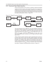
3.2.5 Control and Indicator Circuits
Three main control circuits are provided with the TPA005D12. The mute circuit
grounds the output of the active amplifier, and the shutdown circuit places the
entire device into a power-saving sleep mode to minimize current
consumption. Each of these inputs is TTL compatible: less than 0.8 V applied
to these pins is considered a logic low, and any voltage greater than 2 V is
considered a logic high.
Two indicator pins are also provided for feedback when an under-voltage,
over-current, or thermal fault exists. Module pins are provided for easy
connection of off-board control and monitoring. There are two active low fault
indicator pins on the TPA005D12 amplifier IC (IC pins 40 and 41) that provide
feedback when a fault condition exists. Signals on these pins provide the
status of the class-D amplifier: operational, over-current, thermal fault, and
under-voltage lockout. Table 3–1 lists the possible output conditions of these
pins and a description of the fault indicated.
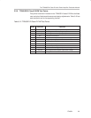
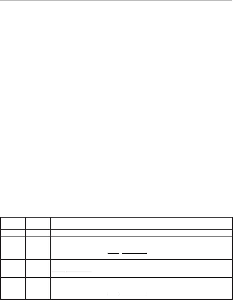
Table 3–1.TPA005D12 Class-D EVM Fault Indicator Table
FAULT 0
(TP 2)
FAULT 1
(TP 3)
DESCRIPTION
1 1 No fault. — The device is operating normally.
1 0 Charge pump under-voltage lockout (VCP-UV) fault — the charge pump voltage is < (PVDD + 6V).
All low-side transistors are turned on, shorting the load to ground. Normal operation resumes when
the charge pump voltage is restored (not a latched fault), however the Fault
indication
remains
active until cleared by cycling MUTE
, SHUTDOWN, or the power supply.
0 1 Over-current fault — the output current limit has been exceeded. All output transistors are switched
off, causing the load to see a high impedance state. This is a
latched
fault and is cleared by cycling
MUTE
, SHUTDOWN, or the power supply.
0 0 Thermal fault — the internal junction temperature has exceeded 125°C. All of the low-side
transistors are turned on, shorting the load to ground. Once the junction temperature drops by 20°C
and is below 125°C, normal operation resumes (not a latched fault). The Fault
indication
remains
active until cleared by cycling MUTE
, SHUTDOWN, or the power supply.