


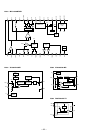

– 52 –
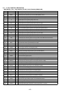
Pin No. Pin Name I/O
Description
80 VB MON I
Un-regulator power supply voltage monitor input terminal (A/D input)
81 CHG MON I
Rechargeable battery voltage monitor input from the MPC18A31FTA (IC901) (A/D input)
82 VREF MON I
Reference voltage monitor input from the SN761056ADBT (IC501) (A/D input)
83 WK DET I
Set key starting detect signal input terminal (A/D input)
84
HALF LOCK
SW
I
Open knob detect switch (S802) input terminal “L”: normal position, “H”: open knob slid
85 RMC KEY I
Remote commander with headphone key input terminal (A/D input)
86 SET KEY 1 I Set key input terminal (A/D input) (
x
,
>
,
.
,VOL +/– keys input)
87 SET KEY 2 I Set key input terminal (A/D input) (
B
, jog, END SEARCH keys input)
88 REC KEY I
REC key input terminal
89 VRM MON I
VREM voltage monitor input terminal (A/D input)
90 HIDC MON I
HI-DC voltage monitor input terminal (A/D input)
91 AD GND — Ground terminal (for A/D converter)
92 AVREF I Input terminal for power supply voltage adjustment reference voltage (+2.4V) (for A/D converter)
93 AVDD —
Power supply terminal (+2.4V) (for A/D converter)
94 TEST0 I
Input terminal for the test (normally: fixed at “L”)
95 TEST1 I
Input terminal for the test (normally: fixed at “L”)
96 TDI I
Input terminal for JTAG Not used (open)
97 TMS I
Input terminal for JTAG Not used (open)
98 TCK I
Input terminal for JTAG Not used (open)
99 TRST I
Input terminal for JTAG Not used (open)
100 TDO O
Output terminal for JTAG Not used (open)
101 TSB CLKCTL O
TSB clock control signal output terminal
102 SSB DATA I/O Two-way SSB serial data bus with the SN761056ADBT (IC501)
103 SSB CLK O SSB serial clock signal output to the SN761056ADBT (IC501)
104 FLASH WR EN —
Not used (fixed at “H”)
105 VDD —
Power supply terminal (+2.4V)
106 VSS — Ground terminal
107 to 109
VLC1 to VLC3 —
Power supply terminal for the liquid crystal display (+2.4V)
110 XCS ADA O
Chip select signal output to the A/D, D/A converter (IC301)
111 XPD ADA O
Power supply control signal output to the A/D, D/A converter (IC301)
112
XRST MTR DRV
O Reset signal output terminal “L”: reset Not used (open)
113 OPT DET I
DIN plug detect signal input terminal
114 XJACK DET I
LINE IN plug detect signal input terminal
115 XMIC DET I
MIC plug detect signal input terminal
116 XOPT CONT O
Power supply control signal output to the DIN plug laser diode
117 MUTE O Analog muting on/off control signal output terminal “L”: muting off, “H”: muting on
118 XHP STBY TMP O
Power supply control signal output to the headphone amplifier Not used (open)
119 XCS NV O
Chip select signal output to the EEPROM (IC802)
120 XINT REC SW O
Not used (open)