


– 48 –
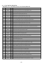
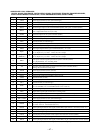
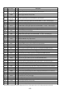
Pin No. Pin Name I/O Description
46 FS256 O Clock signal (11.2896 MHz) output to the A/D, D/A converter (IC301) (X' tal system)
47 to 52
A03, A04, A02,
A05, A01, A06
O Address signal output to the external D-RAM Not used (open)
53 VDIO1
—
Power supply terminal (+2.4V) (for I/O)
54 VSIO1
—
Ground terminal (for I/O)
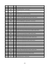
55 to 59
A00, A07, A10.
A08, A09
O Address signal output to the external D-RAM Not used (open)
60 XRAS O Row address strobe signal output to the external D-RAM “L” active Not used (open)
61 IXOE O Output enable signal output terminal for internal D-RAM “L” active Not used (open)
62 IXWE O Data write enable signal output terminal for internal D-RAM “L” active Not used (open)
63 XCAS O Column address strobe signal output to the external D-RAM “L” active Not used (open)
64 to 67 D1, D2, D0, D3 I/O Two-way data bus with the external D-RAM Not used (open)
68 VDC3
—
Power supply terminal (+1.8V) (for internal logic)
69 VSC3
—
Ground terminal (for internal logic)
70 A11 O Address signal output to the external D-RAM Not used (open)
71 XOE O Output enable signal output to the external D-RAM “L” active Not used (open)
72 XWE O Data write enable signal output to the external D-RAM “L” active Not used (open)
73 MVCI I (S) Digital in PLL oscillation input from the external VCO Not used (fixed at “L”)
74 ASYO O (A) Playback EFM full-swing output terminal
75 ASYI I (A) Playback EFM asymmetry comparator voltage input terminal
76 AVD1
—
Power supply terminal (+2.4V) (analog system)
77 BIAS I (A) Playback EFM asymmetry circuit constant current input terminal
78 RFI I (A) Playback EFM RF signal input from the SN761056ADBT (IC501)
79 AVS1
—
Ground terminal (analog system)
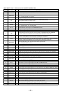
80 PCO O (3) Phase comparison output for master clock of the recording/playback EFM master PLL
81 FILI I (A) Filter input for master clock of the recording/playback EFM master PLL
82 FILO O (A) Filter output for master clock of the recording/playback EFM master PLL
83 CLTV I (A) Internal VCO control voltage input of the recording/playback EFM master PLL
84 PEAK I (A) Light amount signal (RF/ABCD) peak hold input from the SN761056ADBT (IC501)
85 BOTM I (A) Light amount signal (RF/ABCD) bottom hold input from the SN761056ADBT (IC501)
86 ABCD I (A) Light amount signal (ABCD) input from the SN761056ADBT (IC501)
87 FE I (A) Focus error signal input from the SN761056ADBT (IC501)
88 AUX1 I (A) Auxiliary signal (I
3 signal/temperature signal) input terminal Not used (fixed at “H”)
89 VC I (A) Middle point voltage (+1.2V) input terminal
90 ADIO O (A) Monitor output of the A/D converter input signal Not used (open)
91 ADRT I (A) A/D converter operational range upper limit voltage input terminal (fixed at “H” in this set)
92 AVD2
—
Power supply terminal (+2.4V) (analog system)
93 AVS2
—
Ground terminal (analog system)
94 ADRB I (A) A/D converter operational range lower limit voltage input terminal (fixed at “L” in this set)
95 SE I (A) Sled error signal input terminal Not used (fixed at “L”)
96 TE I (A) Tracking error signal input from the SN761056ADBT (IC501)
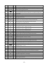
97 DCHG I (A) Connected to the +2.4V power supply
98 APC I (A) Error signal input for the laser automatic power control Not used (fixed at “H”)
99 ADFG I (A) ADIP duplex FM signal (22.05 kHz ± 1 kHz) input from the SN761056ADBT (IC501)
100 VDIO2
—
Power supply terminal (+2.4V) (for I/O)
101 VSIO2
—
Ground terminal (for I/O)
102 F0CNT O Filter f0 control signal output terminal Not used (open)
* I (S) stands for schmitt input, I (A) for analog input, O (3) for 3-state output, and O (A) for analog output in the column I/O