


MZ-R90/R91
– 29 –
– 30 –
– 31 –
– 32 –
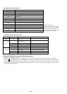
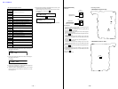
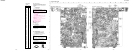
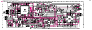
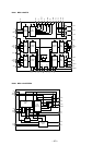
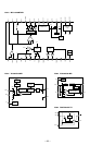
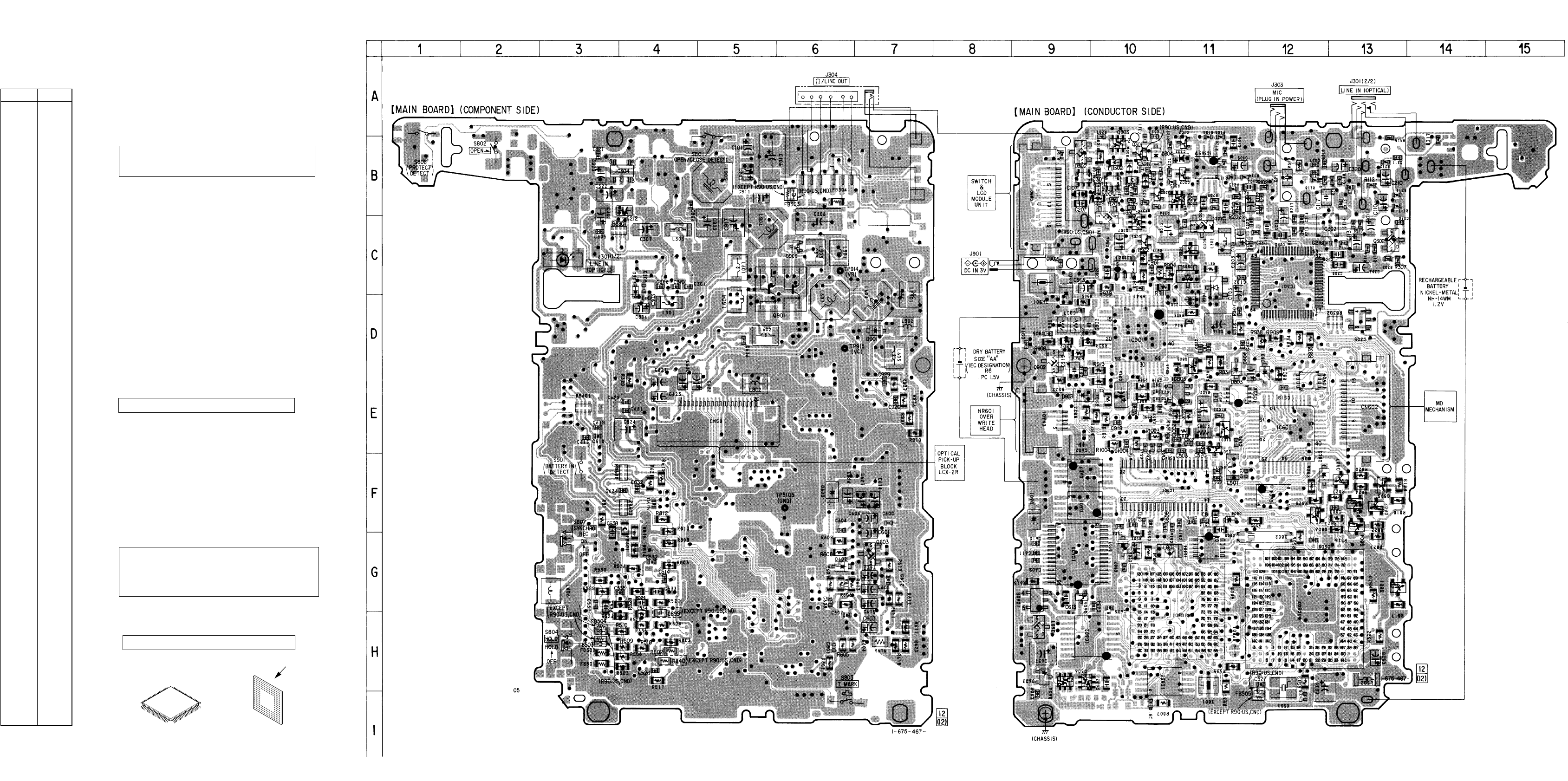
6-4. PRINTED WIRING BOARD
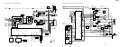
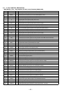
• Semiconductor
Location
Ref. No. Location
D301 B-10
D302 B-9
D303 C-4
D304 B-10
D501 G-10
D600 F-6
D601 F-9
D602 G-6
D603 H-9
D801 E-12
D802 F-12
D803 D-11
D804 F-11
D901 D-7
D902 C-9
D903 E-9
D905 C-11
D906 C-11
D907 D-11
IC301 C-12
IC302 C-13
IC303 B-11
IC304 B-4
IC305 D-13
IC501 F-10
IC502 G-12
IC504 E-11
IC505 E-12
IC601 E-12
IC602 H-9
IC603 G-9
IC604 F-12
IC605 G-9
IC801 H-11
IC802 H-10
IC803 E-11
IC804 G-11
IC901 D-10
IC902 C-10
Q101 B-9
Q102 B-11
Q201 C-10
Q202 B-11
Q301 B-10
Q302 C-13
Q303 B-10
Q305 C-11
Q306 H-9
Q307 C-10
Q308 B-11
Q309 B-10
Q501 E-11
Q601 F-9
Q602 F-9
Q603 G-7
Q604 H-9
Q605 G-9
Q607 H-9
Q801 G-13
Q802 F-13
Q803 F-13
Q804 F-13
Q805 F-13
Q806 F-12
Q807 F-13
Q809 D-11
Q901 C-6
Q902 D-9
Q904 C-11
Q905 C-6
Q906 C-10
Q1001 E-11
• Main board is four-layer printed board.
However, the patterns of layers 2 and 3 have not been in-
cluded in this diagrams.
*
IC502 and IC801 are not replaceable
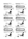
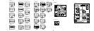
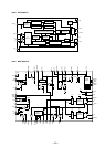
• Lead Layouts
surfac
e
Lead layout of conventional IC CSP (chip size package)
Note on Printed Wiring Board:
• X : parts extracted from the component side.
• Y : parts extracted from the conductor side.
• x : parts mounted on the conductor side.
•
z
: Through hole.
• b : Pattern from the side which enables seeing.
(The other layers' patterns are not indicated.)
Caution:
Pattern face side: Parts on the pattern face side seen from
(Conductor Side) the pattern face are indicated.
Parts face side: Parts on the parts face side seen from
(Component Side) the parts face are indicated.
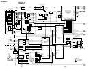
Note on Schematic Diagram:
• All capacitors are in µF unless otherwise noted. pF: µµF
50 WV or less are not indicated except for electrolytics
and tantalums.
• All resistors are in Ω and
1
/
4
W or less unless otherwise
specified.
• % : indicates tolerance.
•
f
: internal component.
• C : panel designation.
• A : B+ Line.
• Power voltage is dc 3 V and fed with regulated dc power
supply from external power voltage jack.
• Voltages and waveforms are dc with respect to ground
under no-signal conditions.
no mark : PLAYBACK
( ) : RECORD
∗
: Impossible to measure
• Voltages are taken with a VOM (Input impedance 10 MΩ).
Voltage variations may be noted due to normal produc-
tion tolerances.
• Waveforms are taken with a oscilloscope.
Voltage variations may be noted due to normal produc-
tion tolerances.
• Circled numbers refer to waveforms.
• Signal path.
E : PLAYBACK (ANALOG OUT)
j : PLAYBACK (ANALOG IN)
l : RECORD (DEGITAL IN)
• Abbreviation
CND : Canadian model
FR : French model
HK : Hong Kong model
JEW : Tourist model
Note: The components identified by mark 0 or dotted line
with mark 0 are critical for safety.
Replace only with part number specified.
*
IC502 and IC801 are not replaceable
• The voltage and waveform of CSP (chip size package) can-
not be measured, because its lead layout is different form
that of conventional IC.
Ver 1.2 2000. 02