


– 22 –
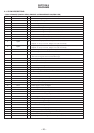
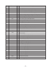
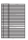
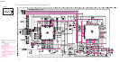
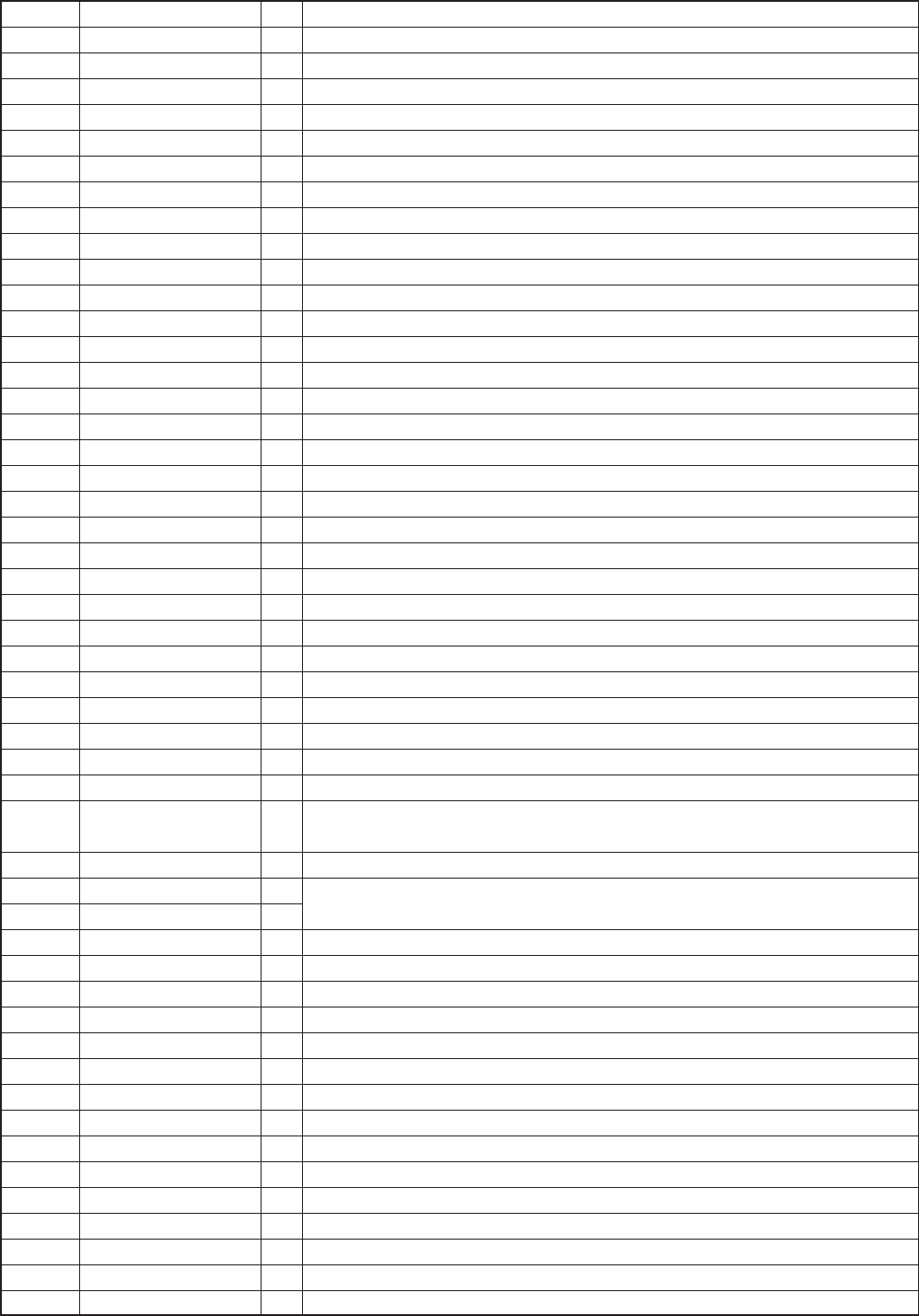
Pin No. Pin name I/O Pin Description
1 CLKCS O Not used (Chip select output to real time clock).
2 XRST O Reset output. L : Reset
3 WRPWR O Laser power switching signal output.
4 TX O Write data transfer timing output.
5 SDI2 I Serial data input.
6 SDO2 O Serial data output.
7 SCK2 O Serial clock output.
8 RFSW O Power control output.
9 SSB I/O SSB data signal input and output.
10 SSB SCK I/O SSB clock signal input and output. (Not used (Open).)
11 DTCK I/O Remote control data signal input/output.
12 SPCK — Not used (Open).
13 WP I Wake-up signal input from remote control key and this unit key.
14 OPEN I Detecting switch for opening and closing of the upper cover. L : Close
15 CLOCK I Not used (CLOCK SET switch input).
16 NI MH CHG O NI MH charge control output.
17 SLEEP O Sleep signal output.
18 T.MARK I T.MARK (Track mark) switch input.
19 REC I Not used (REC switch input).
20 PROTECT I Disc write protect switch. H : Protect
21 HOLD I HOLD switch input (This unit). L : HOLD
22 SYNC REC I SYNCHRO REC switch input.
23 D. B. B I DIGITAL MEGA BASS slide switch input.
24 XLINEDET I LINE IN (OPTICAL) detection input. L : LINE IN
25 INMU1 O INMU signal output.
26 XTEST I Test mode terminal. L : Test mode
27 XDCIN I Not used (Open). (DC input detect. L : DC IN)
28 KANA SE L — Not used (Open).
29 XPHOTO SW O ON/OFF control signal output of PHOTO circuit.
30 XP CONT — Not used (Open). (Power control output. L : ON)
31 X2VCONT —
Not used (Open). (Outputs H while operating with a lithium battery. 2V power control
signal output. L : ON)
32 XREC LED — Not used (Open). (REC LED control. L : ON)
33 MODE2 O
34 MODE1 O
REC drive (IC901) control signal output.
35 XNIMH CHG — Not used (Open). (Battery charger control signal output. L : Charge)
36 XLCD ON O LCD ON/OFF control. L : ON
37 INMU0 O INMU signal output.
38 MRST I Microprocessor reset input.
39 VSS — Ground.
40 XTAL — System clock (12 MHz).
41 EXTAL — System clock (12 MHz).
42 LCD DS O LCD communication strobe signal output to LCD driver.
43 LCD XC D O Com/data select signal output.
44 LCD DATA O LCD data output.
45 LCD SCK O Serial clock output.
46 CHG MNT I Battery charge voltage minitor input.
47 INLS I Detecting switch for internal circuit of sleding. L : Internal circuit
48 HIDC MNT I Voltage monitor DC input.
49 KEY R I Remote control key input.
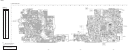
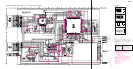
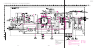
• IC801 CXP740010 (SYSTEM CONTROL)