


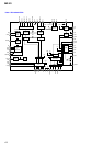
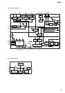
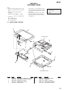
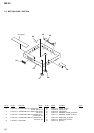
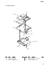
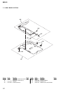
49
MZ-N1
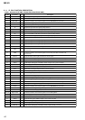
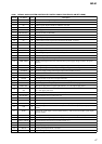
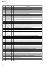
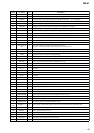
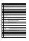
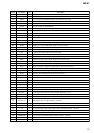
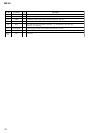
Pin No.
Pin Name
I/O Description
101 XUDP UP ON O Pull-up resistor changeover control signal output of USB data (+) output terminal Not used
102 LCD RST O Reset control signal output to the liquid crystal display element module “L”: reset
103 XMUTE O Analog muting control signal output to the headphone amplifier “L”: muting ON
104 XRST
I
System reset signal input from the power control “L”: reset
105 STAND DET I USB cradle detection signal input terminal
106 VB MON
I
Voltage monitor input terminal (A/D input) of the UNREG power supply
107 CHG MON
I
Charge voltage monitor input (A/D input) from the power control
108 VREF MON I Clear reference voltage monitor input (A/D input) from the RF amplifier
109, 110 SET KEY 1, 2 I Key input terminal (A/D input) from the switch & liquid crystal display element module
111 VBUS DET I USB power supply voltage detection terminal
112 HIDC MON
I
HIGH DC voltage monitor input terminal (A/D input)
113 WK DET
I
Set key and USB start switching detection signal input terminal (A/D input)
114 REC KEY
I
REC key input terminal (A/D input)
115
HALF LOCK
SW
I
Open button detection switch input terminal (A/D input)
Input “L” when the open button is pressed. Input “H” in other cases.
116 RMC KEY
I
Key input terminal (A/D input) from the remote commander attached headphone
117 AVDD
—
Power supply terminal (for the microcomputer analog) (+2.6V)
118 AVSS
—
Ground terminal (for the microcomputer analog)
119 TSMVDD
—
Power supply terminal (for the TSB master communication) (+2.6V)
120 RMC DTCK I/O Serial data input/output with the remote commander attached headphone
121 TSLVDD
—
Power supply terminal (for the I/F to TSB slave) (+1.7V)
122, 123 NC
—
Not used
124 TAT
—
Not used
125 TAN
—
Not used
126 NAR
—
Not used
127 ID0
—
Not used
128 SAK
—
Not used
129 IT0
—
Not used
130 MITY
—
Not used
131 SUSPEND
O
USB suspend signal output terminal Not used
132 USBIFVDD
—
Power supply terminal (for USB I/F) (+3V)
133 UDM I USB data (-) input terminal
134 UDP I USB data (+) input terminal
135 UPUEN O USB pull-up resistor connection control output terminal
136 USBOSCVDD
—
Power supply terminal (for the USB oscillation circuit) (+2.2V)
137 UOSCI I Clock (48MHz) input terminal for the USB
138 UOSCO O Clock (48MHz) output terminal for the USB
139 USBOSCVSS
—
Ground terminal (for the USB oscillation circuit)
140 to
142
MODE1 to 3 O Power supply control signal output for the over write head to the over write head drive
143 HD CON 1 O Over write head control signal output to the over write head drive
144 PBVDD
—
Power supply terminal (+1.7V)
145 HD CON 2 O Over write head control signal output to the over write head drive
146 XTEST I Terminal for test mode set (normally: open) “L”: test mode
147 XCS ADA O Chip select signal output to the A/D converter
148 XPD ADA O Power supply control signal output for the drive to the A/D converter