


47
MZ-N1
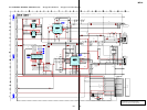
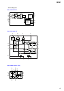
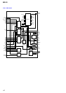
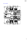
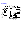
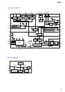
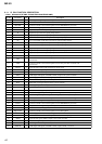
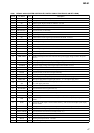
• IC801 CXD2677-202GA (SYSTEM CONTROLLER, DIGITAL SIGNAL PROCESSOR, 16M BIT D-RAM)
Pin No.
Pin Name
I/O Description
1
NC
O
Load address strobe signal output terminal for D-RAM Not used
2
NC
I
Test input terminal for D-RAM Not used
3 to 7
NC
O
Address signal output terminal for D-RAM Not used
8, 9
NC
I/O
Two-way data bus terminal for D-RAM Not used
10, 11
DRAMVDD0, 1
—
Power supply terminal (for D-RAM) (+2.2V)
12, 13
DRAMVSS0, 1
—
Ground terminal (for D-RAM)
14, 15
NC
I/O
Two-way data bus terminal for D-RAM Not used
16 to 19
NC
O
Address signal output terminal for D-RAM Not used
20
NC
O
Column address strobe signal output terminal for D-RAM Not used
21
NC
I
Test input terminal for D-RAM Not used
22, 23
NC
O
Address signal output terminal for D-RAM Not used
24
DVSS0
—
Ground terminal (for the DSP block)
25
DVDD0
—
Power supply terminal (for the DSP block) (+1.1V)
26
OFTRK
I
Off track signal input from the DSP monitor (3)
27
SSB DATA I/O SSB data input/output with the RF amplifier
28
SSB CLK O SSB clock output to the RF amplifier
29
VREC PWM O
PWM signal output for the Over write head drive power supply voltage control to the power
control
30
VL PWM O PWM signal output for the laser power supply voltage control to the power control
31
VC PWM O PWM signal output for the system power supply voltage control to the power control
32
VD PWM O VD power supply voltage control signal output to the DC/DC converter
33
NC
—
Not used
34
IFVDD0
—
Power supply terminal (for the microcomputer I/F block) (+1.7V)
35
IFVSS0
—
Ground terminal (for the microcomputer I/F block)
36
OPT DET I DIN plug detection signal input terminal “H”: DIN plug detect
37
XJACK DET I LINE IN plug detection signal input terminal “L”: LINE or OPT plug detect
38
XMIC DET I Microphone plug detection signal input terminal “L”: microphone plug detect
39
OPEN CLOSE
SW
I
Open/close detection switch of the upper panel input terminal
“L”: when upper panel close
40
SET CODE0 I Input terminal for the set (fixed at “L” in this set)
41
SET CODE1 I Input terminal for the set (open in this set)
42, 43
SET CODE1, 2 I Input terminal for the set (fixed at “L” in this set)
44
XPATCH I Patch function detection terminal “L”: patch function Not used
45
SI0 I Serial data input from the nonvolatile memory and liquid crystal display element module
46
SO0 O
Serial data output to the nonvolatile memory, A/D converter and liquid crystal display element
module
47
SCK0 O
Serial clock signal output to the nonvolatile memory, A/D converter and liquid crystal display
element module
48
XGUM ON I Rechargeable battery detection switch input terminal “L”: rechargeable battery in detect
49
BEEP O Beep sound control signal output to the headphone amplifier
50, 51
TEST1, TEST0 I Input terminal for the main test (normally fixed at “L”)
52
KDO
O
Data output terminal Not used
53
KRB
I
Ready/busy signal input terminal Not used
54
KCLK
O
Clock signal output terminal Not used
55
KCS
O
Chip select signal output terminal Not used