


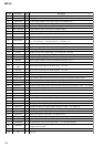
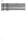
48
MZ-N1
Pin No.
Pin Name
I/O Description
56
KDI
I
Data input terminal Not used
57
TRST
I
Setting terminal for the test mode (normally fixed at “L”)
58
XOPT CTL O Power supply ON/OFF control signal output for the DIN PD drive
59
VG CTL O VG power supply voltage control signal output terminal Not used
60
AOUT SEL O HP/LINE changeover signal output to the headphone amplifier
61
REC OPR LED O LED ON/OFF control signal output for the REC display
62
TSB SSB CTL O TSB/SSB changeover control signal output terminal Not used
63
GND SW2 O Battery for Cradle ON/OFF switch control signal output terminal Not used
64
CLK SEL O System clock select signal output to the power control
65 MIC SENSE O
Mic sensitivity control signal output to the mic amplifier
“L”: Low sensitivity “H”: High sensitivity (normally: “H”)
66 GND SW O GND changeover control signal output terminal
67 XCS LCD O Chip select signal output to the liquid crystal display element module
68 LCD STB O Strobe signal output to the liquid crystal display element module
69 MUTE O Analog muting control signal output “H”: muting ON Not used
70 CS RTC O Chip select signal output to the clock IC
71 XCS NV1 O Chip select signal (1) output to the nonvolatile memory
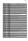
72 IFVDD1
—
Power supply terminal (for the microcomputer I/F block) (+1.7V)
73 IFVSS1
—
Ground terminal (for the microcomputer I/F block)
74
XRST MTR
DRV
O Reset control signal output to the motor driver “L”: reset
75 XRF RST O Reset control signal output to the RF amplifier “L”: reset
76 SPDL MON I Spindle servo monitor signal input
77 XHOLD SW I HOLD switch input terminal “L”: hold ON
78, 79 JOG A, B I Jog dial pulse input terminal from the switch & liquid crystal display element module
80, 81 PD S0, PD S1 O PD IC mode changeover signal output to the optical pick up
82 PAUSE KEY I Pause key input terminal from the switch & liquid crystal display element module
83 PROTECT I Detection input terminal of the record check claw from the protect detection switch “H”: protect
84 SLD MON I Sled servo monitor signal input terminal
85 VLON O Power supply control signal output for the laser diode drive to the power control
86 DVSS1
—
Ground terminal (for the DSP block)
87 DVDD1
—
Power supply terminal (for the DSP block) (+1.1V)
88 SLEEP O System sleep control signal output to the power control “H”: sleep ON
89 FFCLR O Input latch output for the start switching to the power control
90 CHG GAIN O Charge gain control signal output to the power control
91 CHG CTL O Charge ON/OFF control signal output to the power control “H”: charge ON
92 CHGI CTL O Charge current control signal output terminal Not used
93 XHP STBY
O
Power supply control signal output terminal Not used
94 XCS NV2 O Chip select signal (2) output to the nonvolatile memory
95 IFVSS2
—
Ground terminal (for the microcomputer I/F block)
96 IFVDD2
—
Power supply terminal (for the microcomputer I/F block) (+1.7V)
97 T MARK SW I T MARK (track mark) switch input terminal “L”: track mark detection
98 CHG LED O
LED ON/OFF control signal output for CHG (charge display) from the switch & liquid crystal
display element module
99 NC I Initial switch detection input terminal Not used
100 NC
—
Not used