


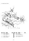
– 62 –
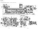
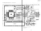
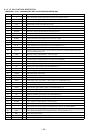
• MAIN BOARD IC501 M30624MG-223FP (SYSTEM CONTROLLER)
Pin No. Pin Name I/O Description
1, 2 NC
O Not used (open)
3C1O
Monitor output terminal for the test C1 error rate is output when test mode
4
ADER
O
Monitor output terminal for the test ADER is output when test mode
5 SQSY
I
Subcode Q sync (SCOR) input from the CXD2656R (IC121)
“L” is input every 13.3 msec Almost all, “H” is input
6 RMC
I Remote control signal input from the remote control receiver (IC761)
7 A1 IN
I Sircs remote control signal input of the CONTROL A1II
8 BYTE
I External data bus line byte selection signal input “L”: 16 bit, “H”: 8 bit (fixed at “L”)
9 CNVSS
— Ground terminal
10 XT-IN
I Sub system clock input terminal (32.768 kHz) Not used (open)
11 XT-OUT
O Sub system clock output terminal (32.768 kHz) Not used (open)
12 S.RST I
System reset signal input from the LA5632 (IC431) and RESET switch (S401) “L”: reset
For several hundreds msec. after the power supply rises, “L” is input, then it changes to “H”
13 XOUT
O Main system clock output terminal (10 MHz)
14 GND
— Ground terminal
15 XIN
I Main system clock input terminal (10 MHz)
16 +3.3V
— Power supply terminal (+3.3V)
17
NMI I Non-maskable interrupt input terminal (fixed at “H” in this set)
18 DQSY
I
Digital In U-bit CD format subcode Q sync (SCOR) input from the CXD2656R (IC121)
“L” is input every 13.3 msec Almost all, “H” is input
19 P.DOWN
I Power down detection signal input terminal “L”: power down, normally: “H”
20
KEYBOARD CLK
I
Keyboard serial clock signal input terminal
21
KEYBOARD DAT
A
I
Keyboard serial data input terminal
22 NC
O Not used (open)
23 XINT
I Interrupt status input from the CXD2656R (IC121)
24 to 26 NC
O Not used (open)
27
KEYBOARD CON
T
O
Keyboard control signal output terminal “H”: off
28 to 30 NC
O Not used (open)
31 SWDT O
Writing data output to the CXD2656R (IC121) and A/D, D/A converter (IC321)
32 SRDT I
Reading data input from the CXD2656R (IC121)
33 SCLK O
Serial clock signal output to the CXD2656R (IC121) and A/D, D/A converter (IC321)
34 FLCS
O Chip select signal output to the FL/LED driver (IC771)
35
FLDATA O Serial data output to the FL/LED driver (IC771)
36 NC
O Not used (open)
37 FLCLK
O Serial data transfer clock signal output to the FL/LED driver (IC771)
38, 39 NC
O Not used (open)
40 ADA LATCH
O Serial data latch pulse signal output to the A/D, D/A converter (IC321)
41 NC
I Not used (fixed at “L”)
42 JOG1
I Jog dial pulse input from the rotary encoder (S713 ≠ AMS ±) (B phase input)
43 JOG0 I
Jog dial pulse input from the rotary encoder (S713 ≠ AMS ±) (A phase input)
44 NC
O Not used (open)
45
A1 OUT O Sircs remote control signal output of the CONTROL A1ΙΙ
46 NC
I Not used (fixed at “H”)
47 NC
O Not used (open)
48 DA RST O
Reset signal output to the A/D, D/A converter (IC321) “L”: reset
49 MUTE O
Audio line muting on/off control signal output terminal “L”: line muting on