– 58 –
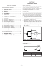
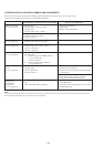
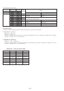
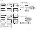
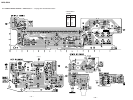
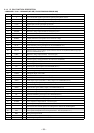
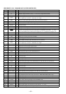
6-14. IC PIN FUNCTION DESCRIPTION
• BD BOARD IC101 CXA2523AR (RF AMP, FOCUS/TRACKING ERROR AMP)
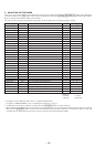
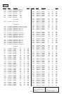
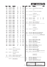
Pin No. Pin Name I/O Description
1II
I-V converted RF signal I input from the optical pick-up block detector
2JI
I-V converted RF signal J input from the optical pick-up block detector
3VCO
Middle point voltage (+1.65V) generation output terminal
4 to 9 A to F I
Signal input from the optical pick-up detector
10 PD I
Light amount monitor input from the optical pick-up block laser diode
11 APC O
Laser amplifier output terminal to the automatic power control circuit
12 APCREF I
Reference voltage input terminal for setting laser power
13 GND —
Ground terminal
14 TEMPI I
Connected to the temperature sensor
15
TEMPR O
Output terminal for a temperature sensor reference voltage
16 SWDT I
Writing serial data input from the CXD2656R (IC121)
17 SCLK I
Serial data transfer clock signal input from the CXD2656R (IC121)
18 XLAT I
Serial data latch pulse signal input from the CXD2656R (IC121)
19 XSTBY I
Standby signal input terminal “L”: standby (fixed at “H” in this set)
20 F0CNT I
Center frequency control voltage input terminal of internal circuit (BPF22, BPF3T, EQ) input
from the CXD2656R (IC121)
21 VREF O
Reference voltage output terminal Not used (open)
22 EQADJ I
Center frequency setting terminal for the internal circuit (EQ)
23 3TADJ I
Center frequency setting terminal for the internal circuit (BPF3T)
24 VCC —
Power supply terminal (+3.3V)
25 WBLADJ I
Center frequency setting terminal for the internal circuit (BPF22)
26 TE O
Tracking error signal output to the CXD2656R (IC121)
27 CSLED I
Connected to the external capacitor for low-pass filter of the sled error signal
28 SE O
Sled error signal output to the CXD2656R (IC121)
29 ADFM O
FM signal output of the ADIP
30 ADIN I
Receives a ADIP FM signal in AC coupling
31 ADAGC I
Connected to the external capacitor for ADIP AGC
32 ADFG O
ADIP duplex signal (22.05 kHz ± 1 kHz) output to the CXD2656R (IC121)
33 AUX O
Auxiliary signal (I
3 signal/temperature signal) output to the CXD2656R (IC121)
34 FE O
Focus error signal output to the CXD2656R (IC121)
35 ABCD O
Light amount signal (ABCD) output to the CXD2656R (IC121)
36 BOTM O
Light amount signal (RF/ABCD) bottom hold output to the CXD2656R (IC121)
37 PEAK O
Light amount signal (RF/ABCD) peak hold output to the CXD2656R (IC121)
38 RF O
Playback EFM RF signal output to the CXD2656R (IC121)
39 RFAGC I
Connected to the external capacitor for RF auto gain control circuit
40 AGCI I
Receives a RF signal in AC coupling
41 COMPO O
User comparator output terminal Not used (open)
42 COMPP I
User comparator input terminal Not used (fixed at “L”)
43 ADDC I
Connected to the external capacitor for cutting the low band of the ADIP amplifier
44 OPO O
User operational amplifier output terminal Not used (open)
45 OPN I
User operational amplifier inversion input terminal Not used (fixed at “L”)
46 RFO O
RF signal output terminal
47 MORFI I
Receives a MO RF signal in AC coupling
48 MORFO O
MO RF signal output terminal