


5
1. SERVICING NOTE .......................................................... 6
2. GENERAL ........................................................................ 16
3. DISASSEMBLY
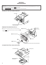
3-1. Case ................................................................................... 19
3-2. Front Panel ......................................................................... 20
3-3. Back Panel ......................................................................... 20
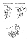
3-4. Main Board and Power Transformer ................................. 21
3-5. CD Mechanism Deck ......................................................... 21
3-6. Tray, Gear and Cam ........................................................... 22
3-7. CD Base Unit ..................................................................... 22
3-8. Optical Pick-up Section of CD (KSS-213BA/F-NP) ......... 22
3-9. BD (CD) Board, Spindle Motor (M101) and
Sled Motor (M102) ............................................................ 23
3-10.MD Mechanism Deck ........................................................ 23
3-11.Slider (Cam) ...................................................................... 24
3-12.Base Unit (MBU-5A) and BD (MD) Board ...................... 24
3-13.Over Write Head ................................................................ 25
3-14.Optical Pick-up of MD (KMS-260B/J1N) ........................ 25
3-15.Spindle Motor (M901) and SLed Motor (M902) (MD) .... 25
4. TEST MODE ..................................................................... 26
5. ELECTRICAL ADJUSTMENTS ............................... 31
6. DIAGRAMS
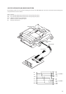
6-1. Circuit Boards Location ..................................................... 40
6-2. Block Diagrams
• BD (CD) Section ............................................................ 41
• BD (MD) Section (1/2) ................................................... 42
• BD (MD) Section (2/2) ................................................... 43
• Main Section ................................................................... 44
6-3. Printed Wiring Board – BD (CD) Section – ...................... 46
6-4. Schematic Diagram – BD (CD) Section – ......................... 47
6-5. Printed Wiring Board – BD (MD) Section – ..................... 48
6-6. Schematic Diagram – BD (MD) Section – (1/2) ............... 49
6-7. Schematic Diagram – BD (MD) Section – (2/2) ............... 50
6-8. Schematic Diagram – SP Section – ................................... 51
6-9. Printed Wiring Board – SP Section – ................................ 51
6-10.Printed Wiring Board – Main Section – ............................ 52
6-11.Schematic Diagram – Main Section – (1/3) ...................... 53
6-12.Schematic Diagram – Main Section – (2/3) ...................... 54
6-13.Schematic Diagram – Main Section – (3/3) ...................... 55
6-14.Schematic Diagram – MD Digital Section – ..................... 56
6-15.Printed Wiring Board – MD Digital Section – .................. 57
6-16.Schematic Diagram – AMP Section – ............................... 58
6-17.Printed Wiring Board – AMP Section – ............................ 59
6-18.Schematic Diagram – Panel Section – ............................... 60
6-19.Printed Wiring Board – Panel Section – ............................ 61
6-20.Schematic Diagram – Power Section – ............................. 62
6-21.Printed Wiring Board – Power Section – ...........................63
6-22.Schematic Diagram – BD Switch Section – ...................... 64
6-23.Printed Wiring Board – BD Swtich Section – ................... 64
6-24.Schematic Diagram – Loading Section – .......................... 64
6-25.Printed Wiring Board – Loading Section –........................ 64
6-26.IC Block Diagrams ............................................................ 65
6-27.IC Pin Functions ................................................................ 69
TABLE OF CONTENTS
7. EXPLODED VIEWS
7-1. Case and Front Panel Section ............................................ 77
7-2. Chassis Section .................................................................. 78
7-3. MD Mechanism Section (MDM-5A) ................................ 79
7-4. MD Base Unit Section (MBU-5A) ....................................80
7-5. CD Mechanism Section (CDM55A-5SBD32)................... 81
7-6. CD Base Unit Section (BU-5SBD32) ............................... 82
7-7. CD Mechanism Section (CDM55C-5BD32)..................... 83
7-8. CD Base Unit Section (BU-5BD32).................................. 84
8. ELECTRICAL PARTS LIST ........................................85
Ver 1.1 2001.06