


Philips Semiconductors
SA5211
Transimpedance amplifier (180 MHz)
Product specification Rev. 03 — 07 October 1998 24 of 28
9397 750 07427
© Philips Electronics N.V. 2001. All rights reserved.
During placement and before soldering, the package must be fixed with a droplet of
adhesive. The adhesive can be applied by screen printing, pin transfer or syringe
dispensing. The package can be soldered after the adhesive is cured.
Typical dwell time is 4 seconds at 250 °C. A mildly-activated flux will eliminate the
need for removal of corrosive residues in most applications.
17.4 Manual soldering
Fix the component by first soldering two diagonally-opposite end leads. Use a low
voltage (24 V or less) soldering iron applied to the flat part of the lead. Contact time
must be limited to 10 seconds at up to 300 °C.
When using a dedicated tool, all other leads can be soldered in one operation within
2 to 5 seconds between 270 and 320 °C.
17.5 Package related soldering information
[1] All surface mount (SMD) packages are moisture sensitive. Depending upon the moisture content, the
maximum temperature (with respect to time) and body size of the package, there is a risk that internal
or external package cracks may occur due to vaporization of the moisture in them (the so called
popcorn effect). For details, refer to the Drypack information in the
Data Handbook IC26; Integrated
Circuit Packages; Section: Packing Methods
.
[2] These packages are not suitable for wave soldering as a solder joint between the printed-circuit board
and heatsink (at bottom version) can not be achieved, and as solder may stick to the heatsink (on top
version).
[3] If wave soldering is considered, then the package must be placed at a 45° angle to the solder wave
direction. The package footprint must incorporate solder thieves downstream and at the side corners.
[4] Wave soldering is only suitable for LQFP, QFP and TQFP packages with a pitch (e) equal to or larger
than 0.8 mm; it is definitely not suitable for packages with a pitch (e) equal to or smaller than 0.65 mm.
[5] Wave soldering is only suitable for SSOP and TSSOP packages with a pitch (e) equal to orlarger than
0.65 mm; it is definitely not suitable for packages with a pitch (e) equal to or smaller than 0.5 mm.
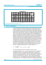
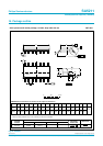
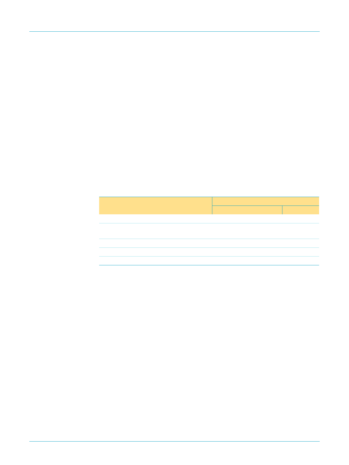
Table 6: Suitability of surface mount IC packages for wave and reflow soldering
methods
Package Soldering method
Wave Reflow
[1]
BGA, HBGA, LFBGA, SQFP, TFBGA not suitable suitable
HBCC, HLQFP, HSQFP, HSOP, HTQFP,
HTSSOP, HVQFN, SMS
not suitable
[2]
suitable
PLCC
[3]
, SO, SOJ suitable suitable
LQFP, QFP, TQFP not recommended
[3][4]
suitable
SSOP, TSSOP, VSO not recommended
[5]
suitable