


Philips Semiconductors
SA5211
Transimpedance amplifier (180 MHz)
Product specification Rev. 03 — 07 October 1998 14 of 28
9397 750 07427
© Philips Electronics N.V. 2001. All rights reserved.
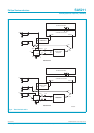
Q
11
– Q
12
which are biased by constant current sources. The collectors of Q
11
– Q
12
are bonded to an external pin, V
CC2
, in order to reduce the feedback to the input
stage. The output impedance is about 17Ω single-ended. For ease of performance
evaluation, a 33Ω resistor is used in series with each output to match to a 50Ω test
system.
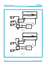
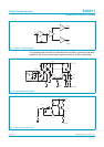
12. Bandwidth calculations
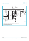
The input stage, shown in Figure 13, employs shunt-series feedback to stabilize the
current gain of the amplifier. A simplified analysis can determine the performance of
the amplifier. The equivalent input capacitance, C
IN
, in parallel with the source, I
S
, is
approximately 4 pF (typical), assuming that C
S
= 0 where C
S
is the external source
capacitance.
Since the input is driven by a current source the input must have a low input
resistance. The input resistance, R
IN
, is the ratio of the incremental input voltage, V
IN
,
to the corresponding input current, I
IN
and can be calculated as:
(2)
Thus C
IN
and R
IN
will form the dominant pole of the entire amplifier;
(3)
Assuming typical values for R
F
= 14.4 kΩ, R
IN
= 200 Ω, C
IN
= 4 pF
(4)
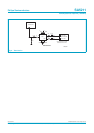
The operating point of Q1, Figure 12, has been optimized for the lowest current noise
without introducing a second dominant pole in the pass-band. All poles associated
with subsequent stages have been kept at sufficiently high enough frequencies to
yield an overall single pole response. Although wider bandwidths have been achieved
by using a cascade input stage configuration, the present solution has the advantage
of a very uniform, highly desensitized frequency response because the Miller effect
dominates over the external photodiode and stray capacitances. For example,
assuming a source capacitance of 1 pF, input stage voltage gain of 70, R
IN
= 60 Ω
then the total input capacitance, C
IN
= (1 + 4) pF which will lead to only a 20%
bandwidth reduction.
13. Noise
Most of the currently installed fiber-optic systems use non-coherent transmission and
detect incident optical power. Therefore, receiver noise performance becomes very
important. The input stage achieves a low input referred noise current (spectral
density) of 1.8 pA/√Hz (typical). The transresistance configuration assures that the
external high value bias resistors often required for photodiode biasing will not
contribute to the total noise system noise. The equivalent input
RMS
noise current is
R
IN
V
IN
I
IN
---------
R
F
1A
VOL
+
-----------------------
14.4 kΩ
71
--------------------
203Ω== = =
f
3db–
1
2πR
IN
C
IN
--------------------------
=
f
3db–
1
2π 4 pF 200 Ω
---------------------------------------
200 MHz==