


Philips Semiconductors
SA5211
Transimpedance amplifier (180 MHz)
Product specification Rev. 03 — 07 October 1998 13 of 28
9397 750 07427
© Philips Electronics N.V. 2001. All rights reserved.
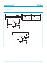
11. Theory of operation
Transimpedance amplifiers have been widely used as the preamplifier in fiber-optic
receivers. The SA5211 is a wide bandwidth (typically 180 MHz) transimpedance
amplifier designed primarily for input currents requiring a large dynamic range, such
as those produced by a laser diode. The maximum input current before output stage
clipping occurs at typically 50µA. The SA5211 is a bipolar transimpedance amplifier
which is current driven at the input and generates a differential voltage signal at the
outputs. The forward transfer function is therefore a ratio of the differential output
voltage to a given input current with the dimensions of ohms. The main feature of this
amplifier is a wideband, low-noise input stage which is desensitized to photodiode
capacitance variations. When connected to a photodiode of a few picoFarads, the
frequency response will not be degraded significantly. Except for the input stage, the
entire signal path is differential to provide improved power-supply rejection and ease
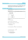
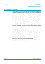
of interface to ECL type circuitry. A block diagram of the circuit is shown in Figure 11.
The input stage (A1) employs shunt-series feedback to stabilize the current gain of
the amplifier. The transresistance of the amplifier from the current source to the
emitter of Q
3
is approximately the value of the feedback resistor, R
F
= 14.4 kΩ. The
gain from the second stage (A2) and emitter followers (A3 and A4) is about two.
Therefore, the differential transresistance of the entire amplifier, R
T
is
(1)
The single-ended transresistance of the amplifier is typically 14.4 kΩ.
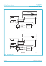
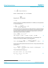
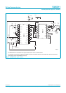
The simplified schematic in Figure 12 shows how an input current is converted to a
differential output voltage. The amplifier has a single input for current which is
referenced to Ground 1. An input current from a laser diode, for example, will be
converted into a voltage by the feedback resistor R
F
. The transistor Q1 provides most
of the open loop gain of the circuit, A
VOL
≈70. The emitter follower Q
2
minimizes
loading on Q
1
. The transistor Q
4
, resistor R
7
, and V
B1
provide level shifting and
interface with the Q
15
– Q
16
differential pair of the second stage which is biased with
an internal reference, V
B2
. The differential outputs are derived from emitter followers
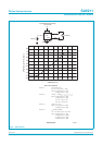
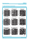
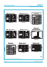
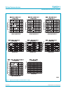
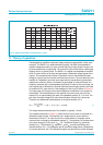
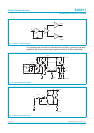
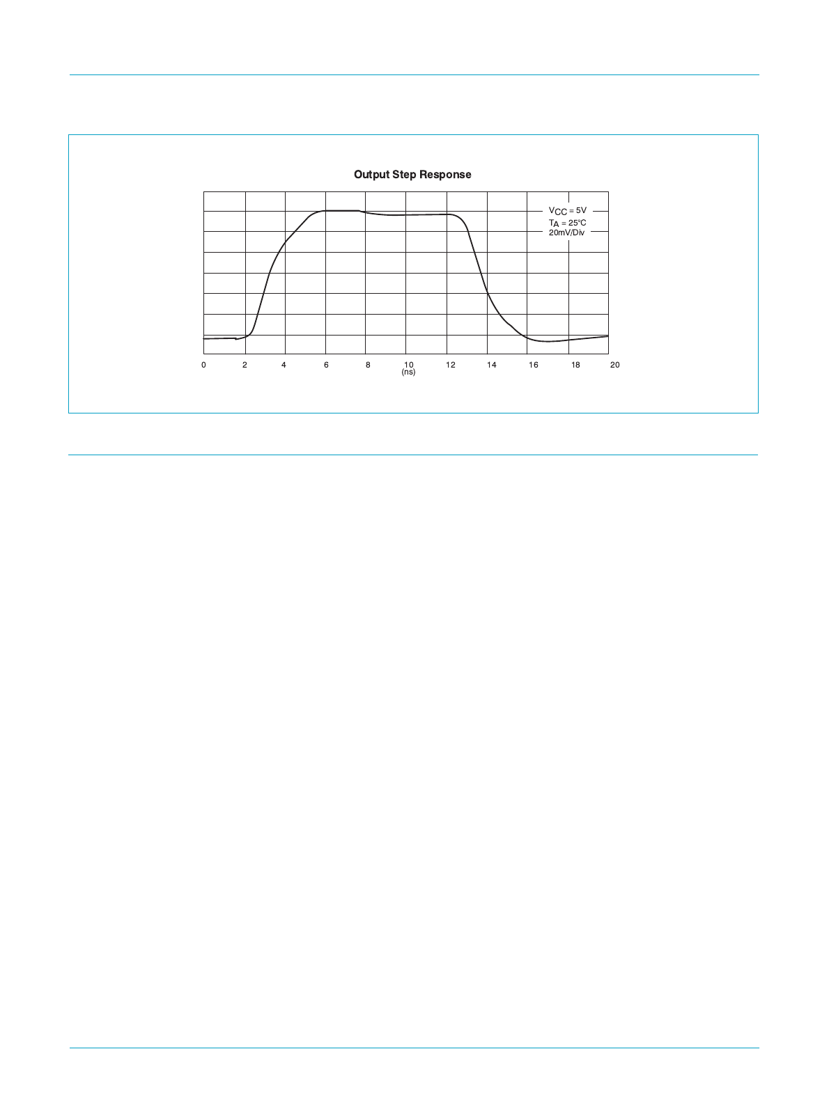
Fig 10. Typical performance characteristics. (cont.)
R
T
V
OUT
diff()
I
IN
----------------------------- 2 R
F
2 14.4 K()28.8 kΩ====