


Philips Semiconductors
SA5211
Transimpedance amplifier (180 MHz)
Product specification Rev. 03 — 07 October 1998 18 of 28
9397 750 07427
© Philips Electronics N.V. 2001. All rights reserved.
15. Application information
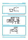
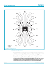
Package parasitics, particularly ground lead inductances and parasitic capacitances,
can significantly degrade the frequency response. Since the SA5211 has differential
outputs which can feed back signals to the input by parasitic package or board layout
capacitances, both peaking and attenuating type frequency response shaping is
possible. Constructing the board layout so that Ground 1 and Ground 2 have very low
impedance paths has produced the best results. This was accomplished by adding a
ground-plane stripe underneath the device connecting Ground 1, Pins 8-11, and
Ground 2, Pins 1 and 2 on opposite ends of the SO14 package. This ground-plane
stripe also provides isolation between the output return currents flowing to either
V
CC2
or Ground 2 and the input photodiode currents to flowing to Ground 1. Without
this ground-plane stripe and with large lead inductances on the board, the part may
be unstable and oscillate near 800 MHz. The easiest way to realize that the part is
not functioning normally is to measure the DC voltages at the outputs. If they are not
close to their quiescent values of 3.3 V (for a 5 V supply), then the circuit may be
oscillating. Input pin layout necessitates that the photodiode be physically very close
to the input and Ground 1. Connecting Pins 3 and 5 to Ground 1 will tend to shield the
input but it will also tend to increase the capacitance on the input and slightly reduce
the bandwidth.
As with any high-frequency device, some precautions must be observed in order to
enjoy reliable performance. The first of these is the use of a well-regulated power
supply. The supply must be capable of providing varying amounts of current without
significantly changing the voltage level. Proper supply bypassing requires that a good
quality 0.1 µF high-frequency capacitor be inserted between V
CC1
and V
CC2
,
preferably a chip capacitor, as close to the package pins as possible. Also, the
parallel combination of 0.1 µF capacitors with 10 µF tantalum capacitors from each
supply, V
CC1
and V
CC2
, to the ground plane should provide adequate decoupling.
Some applications may require an RF choke in series with the power supply line.
Separate analog and digital ground leads must be maintained and printed circuit
board ground plane should be employed whenever possible.
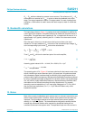
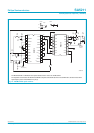
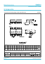
Figure 14 depicts a 50 Mb/s TTL fiber-optic receiver using the BPF31, 850 nm LED,
the SA5211 and the SA5214 post amplifier.