


27
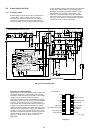
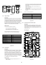
Pin Configuration
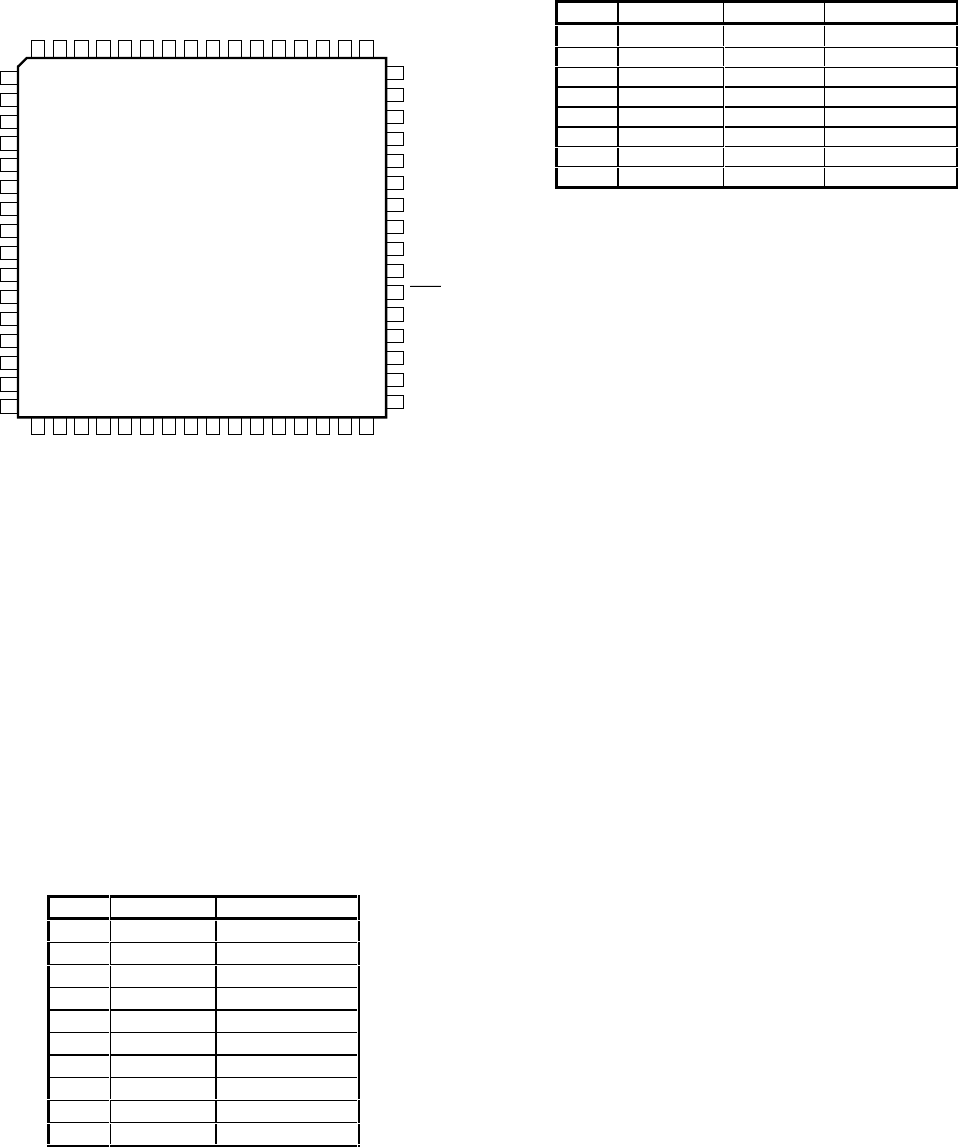
Figure 8-23
8.3.4 TDA7073A Power Drivers (7021, 7022)
Description
The TDA7073A is a dual power driver circuit for servo systems
with a single supply. In this configuration it is used to drive the
sledge, tray, focus and radial.
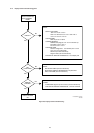
Measurements
Keep microprocessor 7202 in reset by forcing pin 7 of
connector 1208 to +5V. Connect the power supply as
described above in "1.1.1. Supply Voltages". Check the
following voltages :
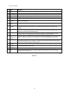
Figure 8-24
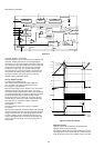
Figure 8-25
8.3.5 BA6856FP Turn Table Motor Driver (7020)
Description
This component is a 3 phase, full wave pseudo linear driving
system with inbuilt Hall Bias circuit and 3 phase parallel output.
Measurements
Keep processor 7202 in reset by forcing pin 7 of connector
1208 to +5V. The outputs 9, 10, 11 of connector 1006 are 0V.
Pin 21 of the motor driver 7020 is 2.5V
± 10%.
Pin 22 of the motor driver 7020 is 2.5V
± 10%.
Pin 23 of the motor driver 7020 is 0V.
Pin 19 of the motor driver 7020 is 5V
± 10%.
Put the processor out of reset to continue the measurement.
Check MOT1 at pin 59 of CD10. The duty cycle of the output
should be 50%. Check wave form at pin 11 of 7005-D :
amplitude 5V + 5% duty cycle 50%.
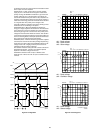
The motor driver 7020 can be measured dynamically by
connecting a hall motor to the application panel. Apply a pulse
of 1V 10Hz and 15% duty cycle to pin 22 (Ec) as input value
with reference to pin 21 (Ecr=2.5V). Measure the output signals
on the driver. This will give as response a square wave on pin
17 and pin 18. When a positive voltage is applied, the square
wave on pin 17 will go ahead of the square wave on pin 18.
All signals will have a value as shown in the truth table. Check
the following output signals :
1
2
3
4
5
6
7
8
9
10
11
12
13
14
15
16
17
18
19
20
21
22
23
24
25
26
27
28
29
30
31
32
33
34
35
36
37
38
39
40
41
42
43
44
45
46
47
48
51
49
50
52
53
54
55
56
57
58
59
60
61
62
63
64
HFREF
HFIN
ISLICE
V
SSA1
V
DDA1
I
ref
V
RIN
D1
D2
D3
D4
R1
R2
V
SSA2
CROUT
CRIN
VDDA2
LN
LP
V
neg
V
pos
RN
RP
SELPLL
TEST1
CL16
RA
FO
SL
DOBM
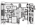
SAA7324
V
SSD3
MOTO1
SFSY
SBSY
RCK
SUB
V
SSD1
V5
V4
V2/V3
KILL
EF
DATA
WCLK
V
DDD1(P)
SCLK
TEST3
CL11/4
RAB
SCLI
TEST2
SDI
WCLI
V
SSD2
SILD
MOTO2
STATUS
V
DDD2(C)
CFLG
V1
RESET
LDON
SDA
SCL
CL96532086_052.eps
080999
Pin Location Value
5 7021
12V
±
10%
5 7022
12V
±
10%
1 7022
1.65V
±
10%
2 7022
1.65V
±
10%
6 7022
1.65V
±
10%
7 7022
1.65V
±
10%
1 7021
5.0
±
10%
2 7021
5.0
±
10%
6 7021
1.65V
±
10%
7 7021
1.65V
±
10%
CL96532086_053.eps
080999
Pin Location Value DC
9 7022 FOC
5.8V
±
10%
12 7022 FOC 5.8V
13 7022 RAD 5.8V
16 7022 RAD 5.8V
9 7021 SLE 5.8V
12 7021 SLE 5.8V
13 7021 TRAY- 5.8V
16 7021 TRAY+ 5.8V
CL96532086_054.eps
080999