


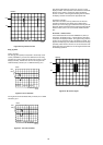
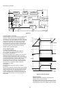
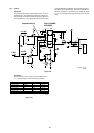
22
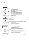
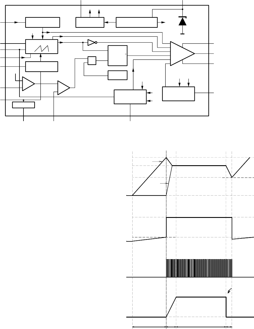
Block diagram of MC44603
Figure 8-13
Operating description of MC44603
The input voltage Vcc (pin 1) is monitored by a comparator with
hysteresis, enabling the circuit at 14.5V and disabling the
circuit below 7.5V. The error amplifier compares a voltage Vfb
(pin 14) related to the output voltage of the power supply, with
an internal 2.5V reference. The current sense comparator
compares the output of the error amplifier with the switch
current Isense (pin 7) of the power supply. The output of the
current sense comparator resets a latch, which is set every
cycle by the oscillator. The output stage is a totem pole,
capable of driving a MOSFET directly.
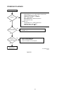
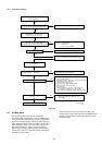
Start up sequence of P816
t1: Charging the capacitors at Vcc
C829 will be charged via R823 and R832, C833 and
C811 via R829. The output is switched off during t1.
t2: Charging of output capacitors
When the input voltage of the IC exceeds 14.5V, the circuit is
enabled and starts to produce output pulses. The current
consumption of the circuit increases to about 17mA, depending
on the external loads of the IC. At first, the capacitors at the Vcc
pin will discharge because the primary auxiliary voltage,
coming from winding 7-9 is below the Vcc voltage. At some
moment during t2, the primary auxiliary voltage reaches the
same level as Vcc. This primary auxiliary voltage now
determines the Vcc voltage.
t3: Regulation
The output voltage of the power supply is in regulation.
t4: Overload
When the output is shorted, the supply voltage of the circuit will
decrease and after some time drop below the lower threshold
voltage. At that moment, the output will be disabled and the
process of charging the Vcc capacitors starts again. If the
output is still shorted at the next t2 phase, the complete start-
and stop sequence will repeat. The power supply goes in a
hiccup mode.
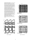
Figure 8-14 ‘Start-up sequence’
Regulation of P816
Figure 8-14 shows the most relevant signals during the
regulation phase of the power supply.
The oscillator voltage ramps up and down between V1 and V2.
The voltage at the current sense terminal is compared every
cycle with the output of the error amplifier Vcomp. The output
VS8 OUT
CONTROL
Dmax &
SOFT-START
Vref
Voc
GND
OUT
VC
PROTECT
VOLTAGE
OVER
MANAGEMENT
OVER
VOLTAGE
DEMAGNETISATION
MANAGEMENT
OSCILLATOR
STANDBY
(REDUCED FREQUENCY)
ERROR
AMP
CURRENT
SENSE
DEMAGNETISATION
DETECT
SYNC INPUT
CT
RF STANDBY
Iref
REFERENCE
BLOCK
SUPPLY
INITIALISATION BLOCK
Vref Iref
Vref
enable
UVL01
VOSC
VOSC PROT
=1
LATCH
THERMAL
SHUTDOWN
BUFFER
VOLTAGE
FEEDBACK
2.5V
RP STANDBY
Iref
UVL01
Vref
FOLDBACK
FOLDBACK
INPUT
CURRENT SENSE
INPUT
SOFT-START
& DMAX
1
2
3
4
6
57 11
8
9
10
15
12
14
13
E/A OUT
16
C
1Set
1Reset
Vstby
CL 96532076_032.eps
290799
1mA
Vo
0
OUTPUT
t4
short
Icc
0V
17mA
14.5V
7.5V
t1
Vcc
p.a.v.
t2 t3
10V
CL 96532076_035.eps
290799