


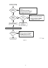

21
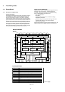
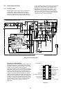
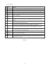
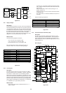
Pin function description
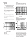
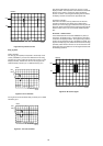
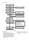
Figure 8-12
Pin Name
Description
1VCC
This pin is the positive supply of the IC. The operating voltage range after start-up is 9.0 to 14.5 V.
2VC
The output high state (VOH) is set by the voltage applied to this pin.
3 Output
Peak currents up to 750 mA can be sourced or sunk, suitable for driving either MOSFET or bipolar transistors.
4Gnd
The groundpin is a single return, typically connected back to the power source.
5 Foldback Input
The foldback function provides overload protection.
6 Overvoltage
Protection
When the overvoltage protection pin receives a voltage greater than 2.5V, the device is disabled and requires a
complete restart sequence.
7
Current Sense
Input
A voltage proportional to the current flowing into the power switch is connected to this input.
8
Demagnetisation
Detection
A voltage delivered by an auxiliary transformer winding provides to the demagnetisation pin an indication of the
magnetisation state of the flyback transformer. A zero voltage detection corresponds to complete core
saturation.
9
Synchronisation
Input
The synchronisation input pin can be activated with either a negative pulse going from a level between 0.7V and
3.7V to Gnd or a positive pulse going from a level between 0.7V and 3.7V up to a level higher than 3.7V. The
oscillator runs free when Pin 9 is connected to Gnd.
10 C
T
The normal mode oscillator frequency is programmed by the capacitor CT choice together with the Rref
resistance value. CT, connected between Pin 10 and Gnd, generates the oscillator sawtooth.
1
1
Soft-
Start/Dmax/Volta
ge-Mode
A capacitor, resistor or a voltage source connected to this pin limits the switching duty-cycle. This pin can be
used as a voltage mode control input. By connecting Pin 11 to Ground, the MC44603 can be shut down.
12 RP Standby
A voltage level applied to the RP Standby pin determines the output power level at which the oscillator will turn
into the reduced frequency mode of operation (i.e. standby mode). An internal hysteresis comparator allows to
return in the normal mode at a higher output power level.
13 E/A Out
The error amplifier output is made available for loop compensation.
14 Voltage
Feedback
This is the inverting input of the Error Amplifier. It can be connected to the switching power supply output
through an optical (or other) feedback loop.
15 RF Standby
The reduced frequency or standby frequency programming is made by the RF Standby resistance choice.
16 Rref
Rref sets the internal reference current. The internal reference current ranges from 100 A to 500 A. This
requires that 5.0k
W £ Rref 25kW.
CL 96532076_031.eps
290799
£