


16
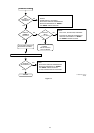
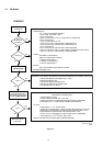
8. Faultfinding Guide
8.1 Display Board
8.1.1 Description of display board
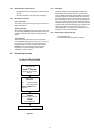
General description
The display board has three major parts : the FTD (Fluorescent
Tube Display), the display controller TMP87CH74F and the
keyboard. The display controller is controlled by the DASP
master processor on the CDR main board. The communication
protocol used is I2C. So all the information between DASP and
display controller goes via the SDA or I2C DATA and SCL or
I2C CLK lines. Communication is always initiated by the DASP
on the CDR main board. Unlike the previous generations of
CDR players, the interrupt generated by the display controller
at key-press or reception of remote control is not used. Instead,
the DASP polls the display controller for these events.
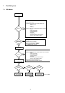
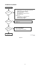
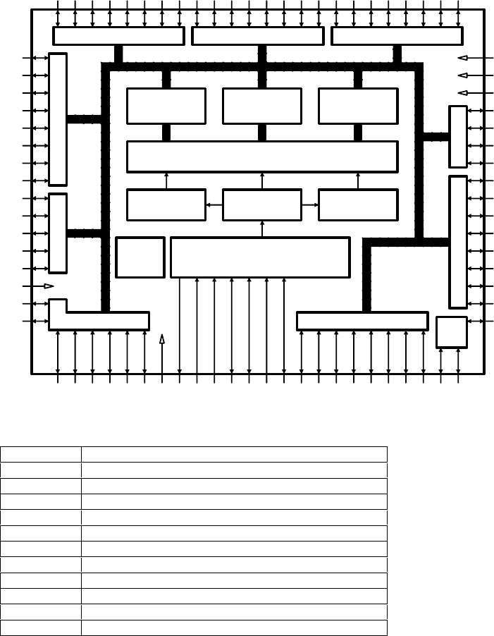
Display controller TMP87C874F
TMP87CH74F ( QY01) is a high speed and high performance
8-bit single chip microprocessor, containing 8-bit A/D
conversion inputs and a VFT (Vacuum Fluorescent Tube)
driver. In this application, its functions are :
slave microprocessor.
FTD driver.
generates the square wave for the filament voltage
required for an AC FTD.
generates the grid and segment scanning for the FTD.
generates the scanning grid for the key matrix.
input for remote control.
All the communication runs via the serial bus interface I2C. The
display controller uses an 8MHz resonator as clock driver.
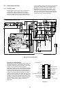
Figure 8-1
651516
26
27
28
29
30
31
32
34
35
36
37
41
141211 17 18 20 21 22
42434445464748495051
10
25
23 244
74
73
72
71
70
69
68
67
66
65
3
64 63 62 61 60 59 58 57 56 55
2
54 53
1
80
79
77
76
75
13
39
38
40
78
79819
33
52
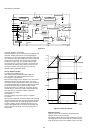
TMP87C874F
SCL
SDA
VSS1
XOUT
XIN
RESETN
P22
P21
TEST1
P20
INT0
INT1
SCK0
PORT3
I C
2
VKK
COUNTER
PROGRAM
I/O PORT1
TIMER/COUNTER
I/O PORT6 (VFT)
VASS
VAREF
VDD
I/O PORT8 (VFT)
CONVERT.
8 BIT A/D
16 BIT
( RAM )
512X8 BIT
DATA MEMORY
TIMER/COUNTER
( ROM )
8kX8 BIT
INTERRUPT
CONTROLLER
I/O PORT7 (VFT)
( I/O PORT2 )
PROGR MEMORY
I/O PORT0
CLOCK/TIMING CONTROLLER
8 BIT
I/O PORTD (VFT) I/O PORT9 (VFT)
I/O PORT5
I/O PORT4
C P U
INT0 external interrupt input 0
INT1 external interrupt input 1
RESETN reset signal input, active low
SCL I2C-bus serial clock input/output
SDA I2C-bus serial data input/output
TEST test pin, tied to low
VAREF analog reference voltage input
VASS analog reference ground
VDD +5V
VKK VFT driver power supply
VSS ground
XIN, XOUT resonator connecting pins for high-frequency clock
BLOCK DIAGRAM
PIN DESCRIPTIONS
CL 96532076_028.eps
290799