


4 - 3
The amplified noise components are converted into the
pulse-type signal at the noise detector section, and output
from pin 13 as the “NOISE” signal. The “NOISE” signal is
applied to the CPU (IC4, pin 47). Then the CPU outputs
“AFON” signal from pin 68 according to the “NOISE” signal
level to toggle the AF power regulator (Q46, Q47) ON and
OFF.
• TONE SQUELCH
The tone squelch detects the tone signal in the demodulated
AF signals, and opens the squelch only when matched sub-
audible tone frequency is detected in the received signal.
While the tone squelch is in use, and the received signal
contains no sub-audible tone signal or mismatched tone
frequency, the tone squelch mutes the AF signals even if the
noise squelch is open.
A portion of the demodulated AF signals from the FM
IF IC (IC15, pin 9) are passed through the two-staged
CTCSS/DTCS fi lter (IC5, pins 5, 7 and pins 1, 2) to suppress
unwanted voice signals. The filtered CTCSS/DTCS signals
are applied to the CPU (IC4, pin 7).
The CPU decodes the CTCSS/DTCS signal, and outputs
“AFON” signal from pin 68 according to the set CTCSS/
DTCS signal to toggle the AF power regulator (Q46, Q47)
ON and OFF.
4-2 TRANSMIT CIRCUITS
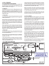
4-2-1 MICROPHONE AMPLIFIER CIRCUIT (MAIN UNIT)
The microphone amplifi er circuit contains AF amplifi er, IDC,
splatter fi lter, etc. The AF signals from the microphone (MIC
signals) are fi ltered and level-adjusted at this circuit.
The AF signals from the microphone are applied to the MIC
amplifi er (IC8, pin 13). The amplifi ed MIC signals are output
from pin 14, and passed through the IDC (Instantaneous
Deviation Control; IC8, pins 8, 9) and splatter fi lter (IC8, pins
5, 7).
The IDC limits the level of the amplitude of MIC signals to
prevent over deviation, and the splatter fi lter suppress 3 kHz
and higher audio components. The fi ltered MIC signals are
passed through the MIC mute switch (Q37) and modulation
volume (Q34).
While receiving, the voltage of R3V line is applied to the
base terminal of the MIC mute switch (Q37) to turn it ON,
thus the MIC line is connected to the ground and the MIC
signals are muted.
The modulation volume (Q34) adjusts the deviation
according to “MODSET” signal from the D/A converter (IC13,
pin 2).
The level adjusted MIC signals are then applied to the
modulation circuit (VCO BOARD; D5 or D6) to modulate the
VCO oscillating signal.
4-2-2 MODULATION CIRCUIT (VCO BOARD)
The modulation circuit modulates the VCO oscillating signal
with the AF signals from the microphone and the tone
signals from the CPU.
• MICROPHONE SIGNALS
The level adjusted MIC signals from the modulation volume
(Q34) are applied to the D5 (in transmitting on 430 MHz
band) or D6 (in transmitting on144 MHz band) to modulate
the VCO oscillating signal by changing the reactance of
D5/D6. The modulated VCO output signal is buffer-amplifi ed
by Q14 and Q19, and applied to the PA BOARD via doubler
switches (D13, D17) and TX/RX switch (MAIN UNIT; D18)
as a transmit signal.
• TONE SIGNALS
The CTCSS and DTCS signals are generated by the CPU
(IC4) and output from pin 141. The CTCSS and DTCS
signals are applied to the modulation circuit (VCO BOARD;
D5 or D6) via the tone fi lter (Q41). To ensure the modulation,
the DTCS signal is also applied to the the reference
frequency oscillator (X2, pin 1), after passing through the
DTCS fi lter (IC8, pins 1, 2) and modulation volume (Q48).
4-2-3 TRANSMIT AMPLIFIERS (PA BOARD)
The VCO output signal is amplifi ed to transmit output power
level by the transmit amplifi ers.
The VCO output signal from VCO BOARD is passed through
the TX/RX switch (MAIN UNIT; D18) and level adjust circuit
(D1), and applied to the pre-driver (Q1), driver (Q2) and
power (Q3) amplifiers in sequence to be amplified to the
transmit output power level. The power amplified transmit
signal is passed through the antenna switching circuit (MAIN
UNIT; D34, D35) and fi lters.
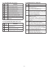
4-2-4 TRANSMIT FILTERS (MAIN UNIT)
The power amplified transmit signal from the PA BOARD
is fi ltered at the transmit fi lters. The transmit fi lters prevent
unwanted RF signals being emitted to the air.
While transmitting on 144 MHz band, the transmit signal is
passed through the LPF (L12, C223, C227), antenna switch
circuit (D35, D38), a couple of LPF (L29, L31, C266, C269,
C276, C283, C514, C516) and HPF (L33, C287, C293), and
two LPFs (L39, L42, C307, C314) before being applied to
the antenna connector (CHASSIS; J1).
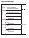
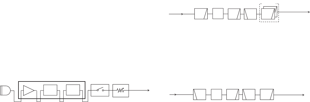
IC8
Q37 Q34
Mic.
13
14
98
MIC mute
Mod. VR
to the VCO
IDC
SPLAT-
TER
MIC
5
7
• MICROPHONE AMPLIFIER CIRCUITS
• 144 MHz
to the antenna
LPF
LPF
LPF
HPF
LPF
from the
PA BOARD
2 LPF’s
D35
ANT
SW
While transmitting on 430 MHz band, the transmit signal
is passed through the HPF (L14, C220, C226), antenna
switching circuit (D34, D37), a couple of LPF (D41, D45, L26,
L30, C255, C257, C262, C275, C282, C289, C515) and HPF
(L38, C302, C306, C310), and the LPF (L42, C314) before
being applied to the antenna connector (CHASSIS; J1).
• 430 MHz
LPF
HPF
LPF
HPF
to the antenna
from the
PA BOARD
D34 D41, D45
ANT
SW