


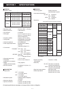
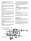
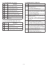
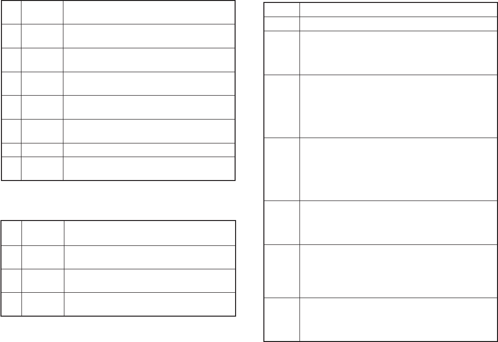
4 - 6
Pin
No.
Port
Name
Description
75 SQL
Input port for [SQL] key (S7).
"Low": While [SQL] is pushed.
76 FUNC
Input port for [FUNC] key (PA BOARD; S1).
"Low": While [FUNC] is pushed.
77 PTT
Input port for [PTT] key. (PA BOARD; S2)
"Low": While [PTT] is pushed.
138 PSET
Outputs transmit power control signal to the
TX power controller (IC17. pin 3).
139 TRAC
Outputs BPFs tracking control signal to the
tracking varactor diodes driver (Q32).
141 CTCOUT Outputs CTCSS/DTCS signal to the MIC line.
144 TEMP
Input port for internal temperature of the
transceiver.
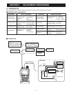
Line Description
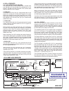
VCC The same voltage as attached battery pack.
CPU3V
Common 3 V converted from VCC line at the
CPU3 regulator (IC11).
The converted voltage is applied to the CPU (IC4),
Re-set IC (IC2), EEPROM (IC1), etc.
+3S
Common 3 V converted from VCCline at the +3S
regulator (Q3, Q4) controlled by "+3SC" signal
from CPU (IC4, pin 53) controlled by "PCON" sig-
nal from the CPU (IC4, pin 52).
The converted voltage is applied to the electric
volume (IC7), VCO BOARD, etc.
+3V
Common 3 V converted from VCCline at the +3V
regulator (IC10, Q1).
The converted voltage is applied to the R3v
regulator (Q6), +10 V DC-DC up-converter (Q7,
Q61, Q62, D3, X4), PLL IC (IC15), D/A converter
(IC13), etc.
R3V
Rceive 3 V controlled by R3V regulator (Q6) using
"R3C" signal from the CPU (IC4, pin 44).
The voltage is applied to the FM IF IC (IC15), 1st
mixer (IC16), 1st IF amplifi er (Q9), RF circuits, etc.
TX3
Transmit 3 V controlled by T3 regulator (Q24-Q26)
using "TXC" signal from the CPU (IC4, pin 54).
The controlled voltage is applied to the TX power
controller IC17, Q31, Q50), pre-driver (PA BOARD;
Q1), microphone amplifi er (IC8), etc.
+10V
Common +10 V boosted at the +10V DC-DC up-
converter (Q7, Q61, Q62, D3, X4).
The boosted voltage is applied to the loop fi lters,
tracking vactor diodes driver (Q32), etc.
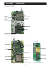
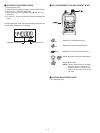
4-4-2 D/A CONVERTER (MAIN UNIT; IC13)
Pin
No.
Port
Name
Description
1 FSET
Outputs reference frequency control signal to
the TCXO (X2, pin 1).
2 MODSET
Outputs modulation level control signal to the
modulation volume circuit (Q37).
3 DTCSET
Outputs DTCS modulation level control signal
to the DTCS modulation volume circuit (Q48).
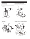
4-5 POWER SUPPLY CIRCUITS
4-4-1 CPU (MAIN UNIT; IC4)-continue