


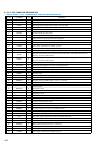
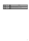
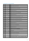
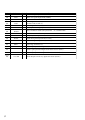
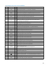
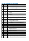
51
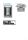
• DIGITAL BOARD IC1401 CXD2712R (AUDIO DSP)
Pin No. Pin Name I/O Description
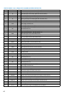
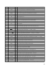
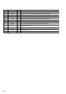
1
VSS3 —
Ground terminal
2 to 5 SOA to SOD O
Serial data output to the A/D, D/A converter
6, 7 ECJ0, ECJ1 I
Conditional jump input terminal (fixed at “L” in this set)
8NCO
Not used (fixed at “L”)
9 XHDWR I
Write data input from the system controller (IC1201)
10 XHDRD I
Read data input terminal Not used (fixed at “H”)
11 VSS4 —
Ground terminal
12 VDD2 —
Power supply terminal (+3.3V)
13 HRDY O
Ready signal output to the system controller (IC1201)
14 XHDCS I
Chip select signal input from the system controller (IC1201)
15
HA0 I
Address signal input from the system controller (IC1201)
16 to 20
HD0 to HD4 I/O
Two-way data bus with the system controller (IC1201)
21
VSS5 —
Ground terminal
22
VDD3 —
Power supply terminal (+3.3V)
23 to 25
HD5 to HD7 I/O
Two-way data bus with the system controller (IC1201)
26
XRST I
Reset signal input from the system controller (IC1201) “L”: reset
27 to 30 FGP0 toFGP3 I/O
Data output terminal for the test
31
VSS6 —
Ground terminal
32 to 40
ED0 to ED8 I/O
Two-way data bus with external RAM Not used (fixed at “L”)
41
VSS7 —
Ground terminal
42 VDD4 —
Power supply terminal (+3.3V)
43 to 49
ED9 to ED15 I/O
Two-way data bus with external RAM Not used (fixed at “L”)
50
TEST I
Test terminal (Normally: fixed at “L”)
51
VSS8 —
Ground terminal
52
VDD5 —
Power supply terminal (+3.3V)
53 to 60
ED16 to ED23 I/O
Two-way data bus with the S-RAM (IC1402)
61
VSS9 —
Ground terminal
62 to 69
ED24 to ED31 I/O
Two-way data bus with the S-RAM (IC1402)
70
XOE O
Output enable signal output to the S-RAM (IC1402)
71
VSS10 —
Ground terminal
72
VDD6 —
Power supply terminal (+3.3V)
73
CAS O
External RAM column address strobe signal output terminal Not used
74
XWE O
Write enable signal output to the S-RAM (IC1402)
75
RAS O
External RAM raw address strobe signal output terminal Not used
76 to 80
EA0 to EA4 O
Address signal output to the S-RAM (IC1402) or test data input from the S-RAM (IC1402)
81
VSS11 —
Ground terminal
82
VDD7 —
Power supply terminal (+3.3V)
83 to 89
E5 to EA11 O
Address signal output to the S-RAM (IC1402) or test data input from the S-RAM (IC1402)
90
EA12 O
Address signal output to the S-RAM (IC1402)
91
VSS0 —
Ground terminal
92 to 94
EA13 to EA15 O
Address signal output to the S-RAM (IC1402)
95
EA16 O
Address signal output terminal (for check)
96
TSTA I
Test data input terminal (Normally: fixed at “L”)
97
PLDIVF I
PLL input frequency select terminal “L”: 256fs “H”: 128fs (fixed at “L” in this set)
98
PLDIVB O
PLL input frequency select terminal “L”: 768fs “H”: 1024fs (fixed at “H” in this set)