


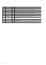

46
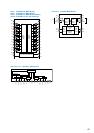
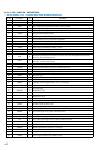
4-32. IC PIN FUNCTION DESCRIPTION
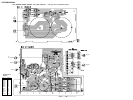
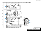
• DIGITAL BOARD IC1101 LC89055W-RA8 (AUDIO INTERFACE RECEIVER)
Pin No. Pin Name I/O Description
1
DISEL I
Input data select terminal (fixed at “L” in this set)
2 DOUT O
EIAJ data and parity output terminal Not used
3 DIN0 I
Amp integrate data input from the select switch (IC1005)
4 DIN1 O
Amp integrate data input terminal Not used (fixed at “L”)
5 DIN2 I
Amp integrate data input terminal Not used (fixed at “L”)
6 DGND —
Ground terminal (digital system)
7 DVDD —
Power supply terminal (+5V) (digital system)
8RI
Input terminal for VCO generator band adjustment
9 VIN I
Input terminal for VCO self running frequency set
10 LPF O
External LPF for PLL is connected to this terminal
11 AVDD —
Power supply terminal (+5V) (analog system)
12 AGND —
Ground terminal (analog system)
13 CK OUT O
Clock signal output to the A/D, D/A converter (IC1503)
14 BCK O
Bit clock signal output to the A/D, D/A converter (IC1503), dolby digital audio decoder
(IC1301), and audio DSP (IC1401)
15
LRCK O
Clock signal output to the A/D, D/A converter (IC1503), dolby digital audio decoder
(IC1301), and audio DSP (IC1401)
16
DATAO O
Audio data output to the dolby digital audio decoder (IC1301)
17
XSTATE O
Clock status flag output to the system controller (IC1201)
18
DGND —
Ground terminal (digital system)
19
DVDD —
Power supply terminal (+5V) (digital system)
20
XMCK O
Not used (open)
21
XOUT O
Clock output terminal Not used (open)
22
XIN I
Clock input from the clock oscillator (IC1404) (12.288MHz)
23
EMPHA O
Emphasis monitor output terminal “H”: on Not used
24
AUDIO O
Terminal for check
25 CSFLAG O
Not used (open)
26 F0/P0/C0 O
Terminal for check
27 F1/P1/C1 O
Terminal for check
28 F2/P2/C2 O
Terminal for check
29 F3/P3/C3 O
Terminal for check
30
DVDD —
Power supply terminal (+5V) (digital system)
31
DGND —
Ground terminal (digital system)
32
AUTO O
Not used (open)
33
BPSYNC O
Not used (open)
34 ERROR O
Error mute output to the system controller (IC1201)
35
DO O
C-bit output to the system controller (IC1201)
36
DI I
Data input from the system controller (IC1201)
37
CE I
Chip enable signal input from the system controller (IC1201)
38
CLK I
Clock signal input from the system controller (IC1201)
39
XSEL I
Clock select terminal (fixed at “H” in this set)
40
MODE0 I
Mode 0 input terminal (fixed at “L” in this set)
41
MODE1 I
Mode 1 input terminal (fixed at “L” in this set)
42
DGND —
Ground terminal (digital system)
43
DVDD —
Power supply terminal (+5V) (digital system)